LMX2615-SP: Question about allowable power rating to ensure we are not stressing the part

Part Number: LMX2615-SP
Other Parts Discussed in Thread: LMK04832

Tool/software:

Hi!

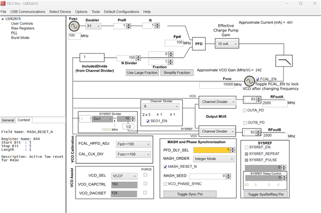
I was able to get an estimate of the current draw of our configuration, but I need some help understanding how to estimate a maximum power rating to show we are not overstressing the part.

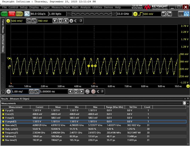
So with our configuration and a Vs max of 3.38V we calculate 3.38V*.491A = 1.6W.

So I was wondering if our ambient temperature is max 55C, could I use PDmax=(TJmaxTA)/θJA -> PDmax=(125°C55°C)/22.7°C/W = 3.08W as an upper limit as to what the part can handle?

I tried doing various settings to find a max current draw, but that doesn't seem like a good way to find a upper limit to the power draw that we can compare against.

For reference we have a .75 derate on our power rating, so if we assume 3.6Vs and 500mA current draw = 1.8W, then after the derate that only allows us 1.3W of power. I feel the actual part can handle more, but Im not sure if the junction temperature is a good way to get a max upper limit or if there are other factors to consider.

  • As an additional question, we technically have a current derate too on the output, but since there are many ways to configure this device is there a way to determine an upper limit on the current output?

  • Hi Arooj,

    I think it is not necessary to find out the max. current consumption configuration. 

    Your requirement (frequency, number of output channel) determines the core current consumption, no matter if the current is high or low, you have to accept it. 

    The only thing you can alternate the total current is the output power setting. Lower setting means lower output power and therefore lower current consumption.

    As we all know, no matter what is the operating conditions, as long as Tj is below the max. rating, the device is safe. Power consumption is one of the factors that determines the Tj. Another factor is the temperature. Here, I recommend use the board temperature (Tb) instead of ambient temperature. This is because most of the heat from the die will transfer to the board as the exposed pad of the device is connected to the board directly. Board temperature is therefore different from ambient temperature. In addition, we can measure board temperature accurately. 

    Tj = ΨJB * Pd + Tb

    In order to reduce the die temperature, pcb stackup and layout also plays an important role. 

    Below appnote have the details of thermal metrics.

    https://www.ti.com/lit/pdf/slua844

    https://www.ti.com/lit/pdf/spra953

    FYI, this is the configuration with the highest current consumption.

  • Thank you for your reply. I believe to show a safe power rating I will use the Tj = ΨJB * Pd + Tb equation you show, and utilize our 90C simulated board temperature. This gives us about 4W of power we can safely dissipate, and with 3.38V and 490mA that's about 1.66W of power and I think that shows we are operating safely below the derated power of 4W*.75 = 3.45W.

    As for the output current, Im starting to think in regards to our parts derating for parts stress it must be more relevant to understand not how much current is consumed by the lmx chip, but rather that the load is not asking too much of the LMX output clocks.


    So we use both outputs to generate two 2500Mhz clocks. RFOUTA goes to the sample clock of a high speed ADC (U8-ADC12DJ3200QML-SP) and RFOUTB goes to FIN on the LMK04832 as the input reference clock. Both RFOUTA and RFOUTB are 50ohm impedance traces.

    The ADC CLK input has an internal 100ohm termination resistor, the LMK FIN0 input impedance seems less defined in the datasheet (we use that part in distribution mode).

    If we assume 100ohm load for RFOUTA and 100ohm load for RFOUTB and the LMX open-collector driver has a 50ohm pullup resistor to 3.3V, then can we calculate that the expected output current is Ioutput=Vswing/Rload​ => Ioutput = 1V/100ohm = 10mA when the transistor is off and the signal is pulled high.

    When the transistor is on, we have measured about 55mA of current through each of those pullup resistors.

    Is there a way to know the current rating of the internal transistors? Since that would be when we draw the most current on the outputs?

  • Hi Arooj,

    LMK04832 CLKin requires external termination for the driver.

    I don't understand the current rating questions, what do you want to figure out?

  • Hi, so RFOUTB goes to FIN0+/- on the LMK part, does that also need an external termination?

    As for the current question. I'm trying to understand if the output power can be converted to an output current value by using the output power to get the voltage swing at the receiver and thereby determine a current draw from the expected load.

    I'm also curious about the fact that this is open collector, so when the transistor is on all the current goes through the internal transistor - and is there a current rating or limit on those transistors?

    Hope that helps?

  • Hi again, I wanted to ping again about the FIN0+/- input pins and if those require external termination?

    Attached is a scope shot of what the clock signal from the LMX look like going into the LMK pins

  • Hi Arooj,

    LMK04832 datasheet suggests use a resistive pad at Fin0 when the input frequency is high.

    From the user's guide, the eval board uses a 3dB pad at each pin.

    I suggest you can copy this design. 

  • If at this point we are unable to make major changes to the design, and we see we meet voltage spec, slew rate, and frequency requirements for our system. If that sufficient to say we can use the design as is? 

  • HI Arooj,

    How did you connect LMX RFoutB and LMK FIN0 together? I don't see that portion in your schematic.

  • Hi Arooj,

    With power setting of 63, I measured RFoutB swing is approx. 1Vpp on a 50Ω load. Your data shown the swing is 1.18Vpp, that means the input impedance of FIN0 is a bit higher than 50Ω. I think this is ok.

  • Thank you for doing this measurement. If it is assumed that we have an input impedance of slightly higher than 50 ohms on each pin, is it safe to say that I can calculate the output power using the following equation with Rload = 100ohms?

  • Hi Arooj,

    Rload here should be 50Ω as our measurement is single-ended.

  • Okay, understood for a single ended measurement it should be 50 ohms, but for a differential measurement it should be 100 ohms correct?

  • Hi Arooj,

    Correct, but V will be doubled in case of differential measurement.