CDCLVP1204: Recommendation for Driving Altera Agilex Differential Input

Part Number: CDCLVP1204

Tool/software:

Hello,

I'm updating a design and I want to connect an unused output from CDCLVP1204 (Vcc = 3.3 V) to a differential clock input on an Altera Agilex 7 FPGA in a 1.2 V bank. It is a 50 MHz clock.

Figure from: Agilex 7 General-Purpose I/O User Guide: F-Series and I-Series, 683780 | 2024.10.07

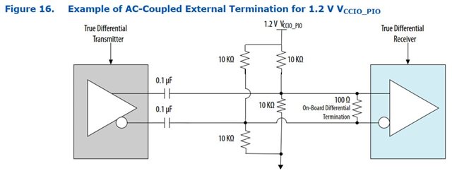
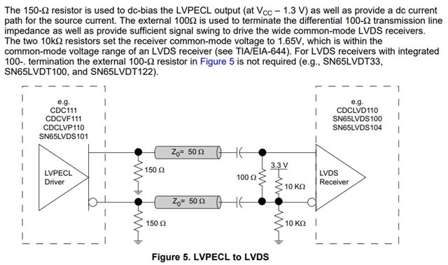
Figure from: TI’s AC-Coupling Between Differential LVPECL, LVDS, HSTL, and CML SCAA059C–2007
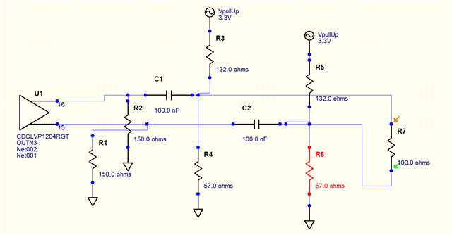

Combined figure:


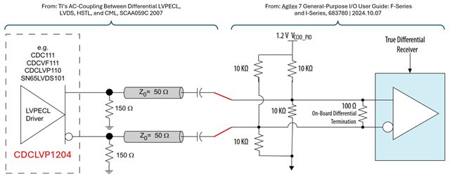
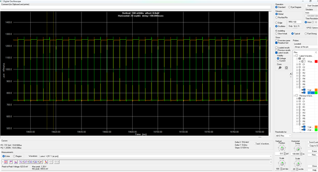
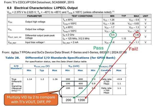
Image showing the numbers don’t work:


Can you provide a recommendation for connecting the two? Perhaps a voltage divider scheme?

Thanks,

Rob

  • Hello Rob sorry for delay. 
    AC coupling to rebias is most easy. 

    We have upcoming device (LMK1U) which is universal buffer with programmable swing and VCM that reduces all the necessary passives since the common mode and power is adjustable via register writes. 
    This would be the most optimal solution as you no longer need to deal with all these terminations, worry about transients, potential reduction in slew rate, decreased PN performance, etc. 

    Best regards, 

    Vicente 

  • Hi Vicente,

    I want to learn how to reduce the peak-to-peak swing at the output of the CDCLVP1204 from 1.35 Vpp to something less than the FPGA's maximum of 1.2Vpp.  I don't understand how your circuit reduces the peak-to-peak swing at the receiver, can you explain or show a simulation plot?

    Thanks,

    Rob

  • Hi Rob, 
    Yes
    The 132 and 57 Ohm termination scheme is what reduces the scheme. 
    Normally LVPECL expects a 50Ohm termination but in this case, I am using 40Ohms to reduce the swing. 
    132 || 57  = ~40
    Here is the plot.


    Best regards, 

    Vicente 

  • Hi Vicente,

    Now I understand, thanks for explaining it.  I consider this resolved.

    Thanks again,

    Rob