LMK04832: Bypass the output of Clockin0 on the LMK04832

Part Number: LMK04832


Tool/software:

Hi,

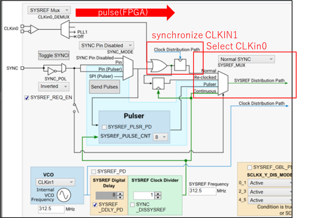
I would like to synchronize the pulse input from Clockin0 with Clockin1 (312.5MHz) on the LMK04832 and output it from Clockout9, 11, and 13.

It seems that the block diagram in TICS.Pro is set up correctly, but the Clockout is always Low. Clockin0 is a signal generated by the FPGA and is being input correctly.

Clockin1 is generating 312.5MHz from a second LMK04832 and is also being input correctly.

The settings are as follows, but is there any additional configuration needed?

R0 (INIT)	0x000080
R0	0x000080
R2	0x000200
R3	0x000306
R4	0x0004D1
R5	0x000563
R6	0x000670
R12	0x000C51
R13	0x000D04
R256	0x010002
R257	0x01010A
R258	0x010280
R259	0x010350
R260	0x010410
R261	0x010500
R262	0x010600
R263	0x010700
R264	0x010804
R265	0x01090A
R266	0x010A80
R267	0x010B50
R268	0x010C10
R269	0x010D00
R270	0x010E00
R271	0x010F00
R272	0x011008
R273	0x01110A
R274	0x011280
R275	0x011350
R276	0x011410
R277	0x011500
R278	0x011600
R279	0x011700
R280	0x011808
R281	0x01190A
R282	0x011A80
R283	0x011B50
R284	0x011C10
R285	0x011D00
R286	0x011E00
R287	0x011F00
R288	0x012008
R289	0x01210A
R290	0x012210
R291	0x012350
R292	0x012420
R293	0x012504
R294	0x012600
R295	0x012710
R296	0x012808
R297	0x01290A
R298	0x012A10
R299	0x012B50
R300	0x012C22
R301	0x012D04
R302	0x012E00
R303	0x012F10
R304	0x013002
R305	0x01310A
R306	0x013210
R307	0x013350
R308	0x013420
R309	0x013504
R310	0x013600
R311	0x013710
R312	0x013840
R313	0x013900
R314	0x013A00
R315	0x013B01
R316	0x013C00
R317	0x013D08
R318	0x013E03
R319	0x013F80
R320	0x0140F2
R321	0x014100
R322	0x014200
R323	0x014300
R324	0x014400
R325	0x014520
R326	0x014618
R327	0x014710
R328	0x014802
R329	0x014902
R330	0x014A02
R331	0x014B06
R332	0x014C00
R333	0x014D00
R334	0x014E00
R335	0x014F7F
R336	0x015000
R337	0x015102
R338	0x015200
R339	0x015300
R340	0x015478
R341	0x015500
R342	0x015696
R343	0x015700
R344	0x015896
R345	0x015900
R346	0x015A05
R347	0x015BD4
R348	0x015C20
R349	0x015D00
R350	0x015E1E
R351	0x015F0B
R352	0x016000
R353	0x016102
R354	0x016241
R355	0x016300
R356	0x016400
R357	0x01650C
R358	0x016600
R359	0x016700
R361	0x016958
R362	0x016A20
R363	0x016B00
R366	0x016E16
R371	0x017360
R375	0x017700
R386	0x018200
R387	0x018300
R388	0x018480
R389	0x018500
R392	0x018800
R360	0x01680C
R1365	0x055500

Thanks.

  • Shunya-san,

    I took a look through your configuration, and it all seems correct - you have CLKin0 going to the SYSREF mux, which is re-clocked through the SYSREF path based on the setting of SYSREF_MUX = 0 and SYNC_MODE = 0. 

    I notice one critical issue - your SYSREF_PD bit is not set. Not setting this bit means that SYSREF is generating a signal based on the 312.5MHz signal that is distributed from CLKin1. By setting this bit, SYSREF_PLSR_PD, and SYSREF_DDLY_PD to 1, you signal to the device that there is no SYSREF signal to be generated internally; but rather, a reclocked signal from CLKin0.

    Thanks,

    Michael

  • Hi, Michael,

    Thank you for your reply.
    I couldn't figure it out by looking at the datasheet, so I decided to repurpose the settings of the LMK04832 that I previously implemented for a completely different purpose, making changes only to the necessary parts.
    As a result, I was able to get it working with the following settings.

    While it is functioning normally, I need to clarify the reasons for its success, so I am comparing the settings.
    Could you please check which registers are responsible for the normal operation?

    Thanks,
    Shunya

    R0 (INIT)	0x000080
    R0	0x000080
    R2	0x000200
    R3	0x000306
    R4	0x0004D1
    R5	0x000563
    R6	0x000670
    R12	0x000C51
    R13	0x000D04
    R256	0x010002
    R257	0x01010A
    R258	0x010290
    R259	0x010360
    R260	0x010400
    R261	0x010524
    R262	0x010600
    R263	0x010701
    R264	0x010808
    R265	0x01090A
    R266	0x010A90
    R267	0x010B40
    R268	0x010C10
    R269	0x010D00
    R270	0x010E00
    R271	0x010F01
    R272	0x011001
    R273	0x01110A
    R274	0x011290
    R275	0x011344
    R276	0x011420
    R277	0x011525
    R278	0x011600
    R279	0x011711
    R280	0x011808
    R281	0x01190A
    R282	0x011A90
    R283	0x011B40
    R284	0x011C20
    R285	0x011D20
    R286	0x011E00
    R287	0x011F11
    R288	0x012008
    R289	0x01210A
    R290	0x012210
    R291	0x012360
    R292	0x012420
    R293	0x012500
    R294	0x012600
    R295	0x012710
    R296	0x012850
    R297	0x01290A
    R298	0x012A10
    R299	0x012B60
    R300	0x012C22
    R301	0x012D04
    R302	0x012E00
    R303	0x012F10
    R304	0x013002
    R305	0x01310A
    R306	0x013200
    R307	0x013340
    R308	0x013420
    R309	0x013500
    R310	0x013600
    R311	0x013710
    R312	0x013840
    R313	0x013900
    R314	0x013A08
    R315	0x013B00
    R316	0x013C00
    R317	0x013D08
    R318	0x013E03
    R319	0x013F00
    R320	0x0140E0
    R321	0x014100
    R322	0x014200
    R323	0x014310
    R324	0x0144FF
    R325	0x014500
    R326	0x014600
    R327	0x014710
    R328	0x014802
    R329	0x014902
    R330	0x014A03
    R331	0x014B06
    R332	0x014C00
    R333	0x014D00
    R334	0x014E00
    R335	0x014F7F
    R336	0x015000
    R337	0x015102
    R338	0x015200
    R339	0x015300
    R340	0x015478
    R341	0x015500
    R342	0x015696
    R343	0x015700
    R344	0x015896
    R345	0x015900
    R346	0x015A05
    R347	0x015BD4
    R348	0x015C20
    R349	0x015D00
    R350	0x015E1E
    R351	0x015F0B
    R352	0x016000
    R353	0x016101
    R354	0x016220
    R355	0x016300
    R356	0x016400
    R357	0x01657D
    R358	0x016600
    R359	0x016700
    R361	0x016958
    R362	0x016A20
    R363	0x016B00
    R366	0x016E16
    R371	0x017370
    R375	0x017700
    R386	0x018200
    R387	0x018300
    R388	0x018480
    R389	0x018500
    R392	0x018800
    R360	0x01687D
    R1365	0x055500
    

  • Shunya-san,

    I am a bit backlogged on bandwidth today. I will be able to look through these registers tomorrow.

    Thanks,

    Michael

  • Michael-san,

    How is the situation regarding this matter?

    I don't quite understand from the datasheet, so I would appreciate it if you could get in touch.

    Thanks,

    Shunya

  • Shunya-san,

    The text file you shared indicates that you have configured the device in distribution mode. 

    This is done by configuring the CLKin1_OUT_MUX in register 0x147 for Fin mode - where the input to CLKin1 is treated as an external VCO and the signal is sent to the output dividers. 

    Thanks,

    Michael

  • Michael-san,

    Register 0x147 is identical before and after the modification; its value is 0x014710.

    What was the reason it did not work before the fix?

    Shunya

  • Shunya-san,

    I misread your configuration file, my apologies. 

    I have gone through and marked what was updated, and I will be reading through the datasheet to provide a root cause tomorrow.

    Thanks,

    Michael