CDCLVC1310: Circuit Design Related Questions

Part Number: CDCLVC1310
Other Parts Discussed in Thread: AM6421,

Hello, We are using CDCLVC1310 clock buffer in one of our designs which is based on AM6421 processor. While refering to EVM schematic "PROC101C(004)_SCH", we found some hardware circuit related queries for CDCLVC1310 on page# 31. Please refer snapshot along with EVM schematic for your reference:

1) Why did we use voltage devider (R255 & R245) at the output of XO (25MHz - U71)?

2) Why we have used Overdrive (Ac-coupling) mode for a path from XO (25MHz - U71) to Clock buffer (CDCLVC1310RHBR - U70)?

As far as i know, if we are using CMOS output XO (25MHz - U71), it is good to use Bypass mode instead of Overdrive mode. Correct me if i am missing something here. Is there any specific rationale here to use Overdrive (Ac-coupling) mode?

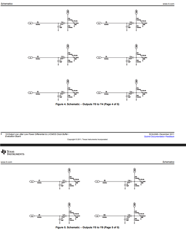
3) At clock buffer output, there are parallel RC dampling networks (C262 & R65 etc.) for Y5 to Y9 only. Why isn't the same is used for Y0 to Y4?

Regards,

Nikhil Jadhav

PROC101C(004)_SCH.pdf 

Screenshot 2025-10-24 103700.png

  • Hello Nikhil, 
    1. The resistor divider network is used to bias the input to VDD/2 in the case of AC coupled input such as Sine wave to ensure 50% duty cycle. 

    2. The reason the XTAL overdrive network is used here is to drive the XTAL. 

    Refer to table 1 and the footnotes at the bottom. 
    You can go use the XTAL directly or you can bypass the XTAL as well. 

    You can also refer to schematic. 

    You're correct, if your input is just an LVCMOS signal you can input this directly to XIN without needing to AC couple. 

    Refer to pages 10-14 for more info. 

    Though if you want to fan out an LVCMOS signal, we have a much more newer capable part which is LMK1C110x family. The temperature range, size, noise floor and additive jtiter are superior. The only thing LMK1C110x family does not offer is ability to use XTAL input or differential input, which both do not matter in your use case if you're already using an LVCMOS input. 

    I don't follow you statement about the placeholder for the passive components on the output side? All outputs have a series placeholder followed by a shunt placeholder followed by another series placeholder which allows for AC coupling followed by the biasing network? This is true for all outputs. 


    Best regards, 

    Vicente 

  • Hello Vicente,

    Thanks for the response. Please help to answer my follow up queries below:

    1. The resistor divider network is used to bias the input to VDD/2 in the case of AC coupled input such as Sine wave to ensure 50% duty cycle.

    Query: Can't we use 1.8V (LVCMOS/CMOS output) XO here directly instead of "using 3.3VDD XO and making it VDD/2". Why do we need to use voltage divider here? Can we bypass voltage divider if we use 1.8V LVCMOS XO?

    2. The reason the XTAL overdrive network is used here is to drive the XTAL. 

    Refer to table 1 and the footnotes at the bottom. 
    You can go use the XTAL directly or you can bypass the XTAL as well. 

    You can also refer to schematic.

    You're correct, if your input is just an LVCMOS signal you can input this directly to XIN without needing to AC couple. 

    Refer to pages 10-14 for more info.

    Query: Thanks for confirmation. Can we skip voltage divider as well if we use bypass mode with same XO (3.3V)?

    Though if you want to fan out an LVCMOS signal, we have a much more newer capable part which is LMK1C110x family. The temperature range, size, noise floor and additive jtiter are superior. The only thing LMK1C110x family does not offer is ability to use XTAL input or differential input, which both do not matter in your use case if you're already using an LVCMOS input. 

    Query: Thanks for your suggestion. We will look into this.

    I don't follow you statement about the placeholder for the passive components on the output side? All outputs have a series placeholder followed by a shunt placeholder followed by another series placeholder which allows for AC coupling followed by the biasing network? This is true for all outputs. 

    Query: As per EVM schematic "PROC101C(004)_SCH (AM64x/AM243x EVM BOARD)" page# 31, at clock buffer (CDCLVC1310RHBR - U70) output, there are parallel RC networks/shunt placeholders (C262 & R65 etc.) for Y5 to Y9 outputs only but this parallel RC networks are not used for Y0 to Y4 outputs of clock buffer? Is there any rationale for this? I have attached EVM schematic and circuit snapshot in my first query message.

    Regards,

    Nikhil Jadhav

  • Hello Vicente,

    Thanks for the response. Please help to answer my follow up queries below:

    1. The resistor divider network is used to bias the input to VDD/2 in the case of AC coupled input such as Sine wave to ensure 50% duty cycle.

    Query: Can't we use 1.8V (LVCMOS/CMOS output) XO here directly instead of "using 3.3VDD XO and making it VDD/2". Why do we need to use voltage divider here? Can we bypass voltage divider if we use 1.8V LVCMOS XO?

    2. The reason the XTAL overdrive network is used here is to drive the XTAL. 

    Refer to table 1 and the footnotes at the bottom. 
    You can go use the XTAL directly or you can bypass the XTAL as well. 

    You can also refer to schematic.

    You're correct, if your input is just an LVCMOS signal you can input this directly to XIN without needing to AC couple. 

    Refer to pages 10-14 for more info.

    Query: Thanks for confirmation. Can we skip voltage divider as well if we use bypass mode with same XO (3.3V)?

    Though if you want to fan out an LVCMOS signal, we have a much more newer capable part which is LMK1C110x family. The temperature range, size, noise floor and additive jtiter are superior. The only thing LMK1C110x family does not offer is ability to use XTAL input or differential input, which both do not matter in your use case if you're already using an LVCMOS input. 

    Query: Thanks for your suggestion. We will look into this.

    I don't follow you statement about the placeholder for the passive components on the output side? All outputs have a series placeholder followed by a shunt placeholder followed by another series placeholder which allows for AC coupling followed by the biasing network? This is true for all outputs. 

    Query: As per EVM schematic "PROC101C(004)_SCH (AM64x/AM243x EVM BOARD)" page# 31, at clock buffer (CDCLVC1310RHBR - U70) output, there are parallel RC networks/shunt placeholders (C262 & R65 etc.) for Y5 to Y9 outputs only but this parallel RC networks are not used for Y0 to Y4 outputs of clock buffer? Is there any rationale for this? I am also attaching EVM schematic pdf and circuit snapshot again below for your quick reference.

    0247.PROC101C(004)_SCH.pdf

    Regards,

    Nikhil Jadhav

  • Hi Nikhil,

    Query: Can't we use 1.8V (LVCMOS/CMOS output) XO here directly instead of "using 3.3VDD XO and making it VDD/2". Why do we need to use voltage divider here? Can we bypass voltage divider if we use 1.8V LVCMOS XO?

    If your clock source is an LVCMOS XO and your VDD is 2.5V, then yes, you may bypass the bias network and input your 1.8V LVCMOS clock directly into the device. Otherwise, it must be AC coupled and rebiased to ensure that VIH and VIL are satisfied for the device.

    Query: Thanks for confirmation. Can we skip voltage divider as well if we use bypass mode with same XO (3.3V)?

    What do you mean by bypass mode? If the signal is appropriately biased (i.e. swings from GND to VDD), then yes, you may skip the voltage divider.

    Query: As per EVM schematic "PROC101C(004)_SCH (AM64x/AM243x EVM BOARD)" page# 31, at clock buffer (CDCLVC1310RHBR - U70) output, there are parallel RC networks/shunt placeholders (C262 & R65 etc.) for Y5 to Y9 outputs only but this parallel RC networks are not used for Y0 to Y4 outputs of clock buffer?

    This has been DNI'ed for all outputs besides Y5. This network serves as a load that would reduce the output slew rate of the device. The one for Y5 can be DNI'ed as well, if the output satisfies the input requirements of the next device.

    Thanks,

    Michael

  • Hello Michael,

    Thanks for the response.

    I am looking into datasheet for VIH and VIL levels for clock input. I found these levels for Primary and Secondary clock inputs but not for XIN. Can you please help with these levels for XIN?

    Regards,

    Nikhil Jadhav

  • Hi Nikhil,

    Please see the footnote of the attached screenshot below.

    The maximum input signal swing and rise time have been specified - as well as the fact that the device may not need AC parameters for the XTAL input. See a screenshot below of the table just above it:

    This indicates the drive level and equivalent series resistance. See the crystal oscillator section for more information.

    Thanks,

    Michael