Part Number: LMX2694EPEVM
Hello E2E experts,
We have procured an LMX2694EPEVM evaluation board for prototyping.
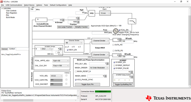
We would like to test SYSREF mode, as indicated in the user manual (p8 figures 9 and 10), by generating a signal on RFOUT B with a programmable delay (relative to RFOUT A), but we are unable to generate this output signal. Figure 10 does not show the signal frequency either (are we really at 100MHz output? With an OSCIN also at 100MHz?).
Our problem is that when we reproduce the PLL settings shown in Figure 9 as example, as soon as VCO_PHASE_SYNC is activated, the RFOUT A output unlocks (the output frequency is no longer 100MHz). The RFOUT B output remains off (no signal). Pressing ‘toggle SysRefFreq Pin’ or ‘Toggle Sync Pin’ causes the USBtoANY module to send only a high state (rising edge) but seems to have no effect on the RFOUT A and RFOUT B outputs.
Can you confirm the hardware configuration and specify whether an external signal is required on the SYNC pin and/or SYSREF? (if the USBtoANY module is sufficient for this case).
Can you send us a configuration file for all the registers to ensure that the test is reproducible?
If possible, please show us a timing diagram for the SYNC, SYSREF, RFOUTA and RFOUTB signals so that we can validate our setup.
Regards,
TICSC