LMKDB1202: schematic review

Part Number: LMKDB1202

Hi,

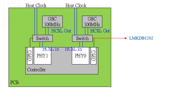
We needs to support switching between SRIS and CC modes at the system level.

The oscillator is 100 MHz with HCSL output, and the PHY uses a 100 MHz HCSL input.

Would you please review below application and shcematic? thanks!

image.png

100MHz OSC Output Spec.

image.png

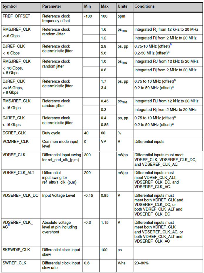
PCIe Phy RefCLK Input Spec
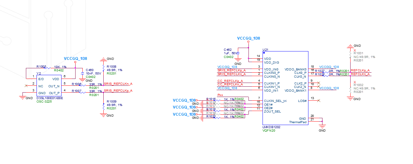
image.png

Schematic:

image.png

Jeff

  • Hi Jeff, 
    Given outputs on LMKDB is LP-HCSL, you don't need placeholder for 50Ohm to GND termination on the outputs. 
    I don't see the VDD filtering network - please check DS section 10.3 for more info. 

    Best regards, 

    Vicente 

  • Hi Vicente,

    Got it, thanl you!

    Jeff

  • Hi Vicente,

    Could you confirm whether this component is already the best fit for the application, or if there is a more suitable option available?
    Does the LMKDB1202 meet the specifications we provided for the OSC output and PHY input?

    Thanks!

    Jeff

  • Hi Jeff, 
    This varies by customer application. 
    Buffer has a noise floor and a certain amount of additive jitter. 
    The main culprit here is the ref clk. 

    The XO has an RMS jitter of 0.1ps 
    The Rx accepts up to 1ps. 

    Buffers will provide a certain amount of additive jitter for a certain integration band - we can also calculate the output jitter in this case. 
    I don't expect LMKDB to provide 0.9ps of jitter. 
    Should be okay for your application but customer can use PLLatinumSim to estimate output PN from the XO if they have a .txt file of the phase noise profile of that device and estimate time domain jitter. 


    Best regards, 

    Vicente