This thread has been locked.

If you have a related question, please click the "Ask a related question" button in the top right corner. The newly created question will be automatically linked to this question.

LMK3H0102-Q1: Orderable part number

Part Number: LMK3H0102-Q1

Hi Team,

We are planning to use the LMK3H0102-Q1 in our design. Our requirements specify that OUT0 and OUT1 should be 100MHz LP-HCSL (100 ohm) outputs, and the part must be automotive grade.
 
We intend to support both VDD and VDDO at 1.8V. The datasheet mentions that the VDDO pins must be the same voltage as VDD.
  1. We are planning to use the LMK3H0102T07RGTRQ1 in this design. Could you please confirm if we can use a VDD of 1.8V for this specific part?
    I noticed that the datasheet also lists dedicated 1.8V variants, such as the LMK3H0102T18 and LMK3H0102TV1, can you just tell the pre configured orderable part number for 100MHz LP-HCSL (100 ohm) outputs with VDDO and VDD as 1.8V, for the specific 1.8V part supported.
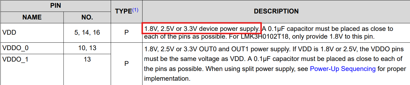
image.png

2.  Currently we set the LMK3H0102T07RGTRQ1 part to OTP Page 0 mode.
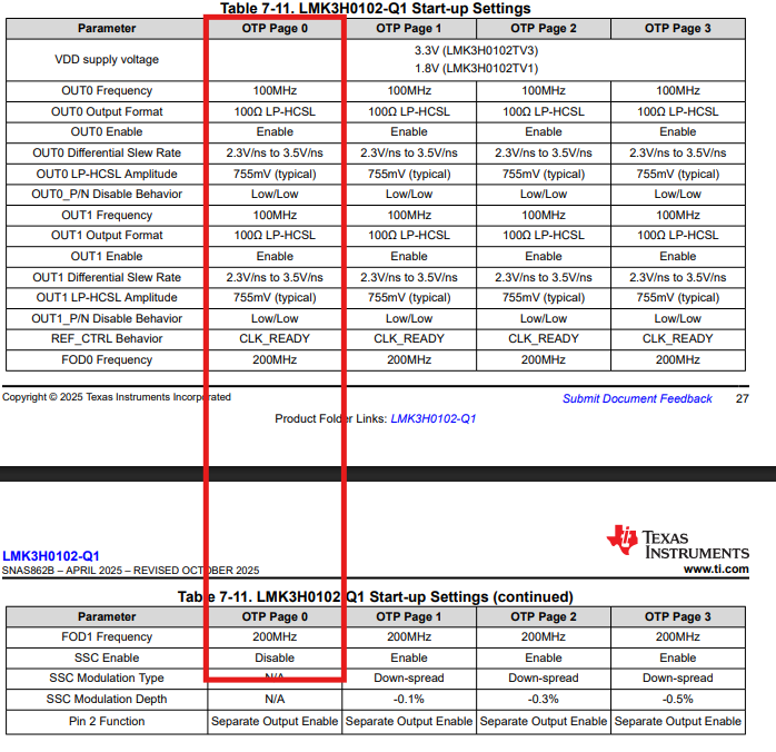
image.png

3. But, LMK3H0102-Q1 part supports default configuration part numbers www.ti.com/.../snau290.pdf

4. Regarding the document mentioned above, I noticed that while several OTP page pre-configuration parts are listed, only one part supports a VDD of 1.8V.Currently, on that part the 100ohm LP-HCSL is disabled by default in this configuration. We would like default enabled part.
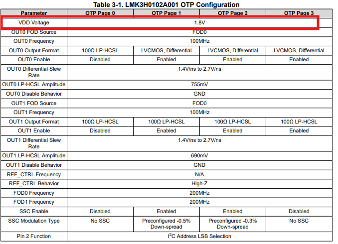
image.png

5. Can we use LMK3H0102A014, why because LMK3H0102A014 part support 100E LP-HCSL in OTP Page 2 Mode but it mentioend VDD as 3.3V can we use LMK3H0102A014  part VDD as 1.8V?
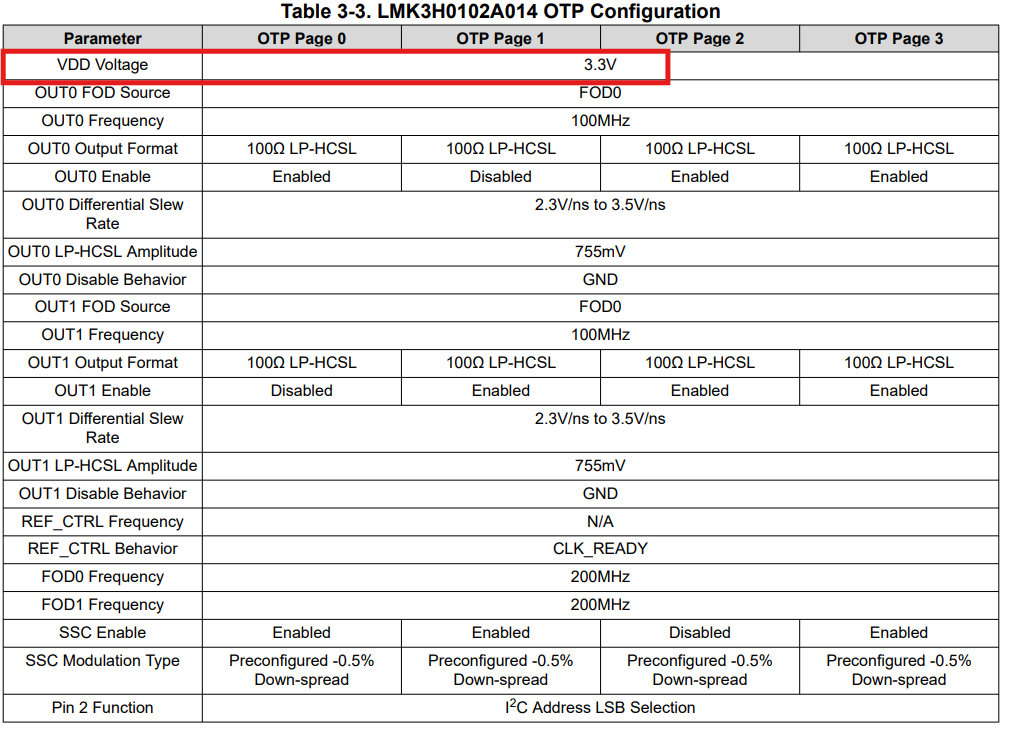
image.png

5. Can you suggest the default configuration part number for below mentioend requirement,

    * Output should be 100ohm LP-HCSL with 100MHz for OUT0 and OUT1.

    * VDD and VDDO should be 1.8V.

    * Automotive grade part.

   * We want single Output Enable (OE)  to control OUT0 and OUT1.

6. We previously used LMK3H0102A010 part, but this pre program configration details are not available in the default configuration document can you just tell those details.

  • Hi,

     we will get back to you by early next week 

    Best,

    Sandra 

  • Hi Praven, 

    Based on the requirements you've outlined, it looks like the LMK3H0102TV1 fits your application in OTP page 0 as long as you have I2C access. I2C can be used to overwrite the OTP settings to configure a single output enable pin for OUT0 and OUT1 via register R11.

    If you need a custom configuration, feel free to reach out to your sales representative and they should be able to assist you further. In reference to your other questions:

    • The LMK3H0102A014 and LMK3H0102T07 can only be supplied on 3.3V VDD
    • We don't have a LMK3H0102A010 part, are you referring to the LMK3H0102A001?

    Best,

    Jaryd

  • Thanks Jaryd Dukes,

    We are planning to use the LMK3H0102TV1RGTRQ1 in our current design and have a few technical queries regarding this IC:
    1. We require a pre-programmed output of 100MHz (LP-HCSL). We plan to use OTP Page 0 to set this as the default, as referenced on page 27 of the datasheet. Please confirm if this is the correct approach.
    2. Since we do not need to program the output dynamically, we do not intend to support an I2C instance for this part.
    3. In this configuration, the OE pin will act as the enable for OUT0 and OUT1. We understand that in OTP mode, the FMT_ADDR pin can set the output format, function as the output enable for OUT1, or have no function. What is the default OTP mode for this pin? Note: We are not supported I2C.
    4. If the FMT_ADDR pin is configured to act as the OUT1 enable, can we tie the OE and FMT_ADDR pins together to enable both outputs simultaneously?
    5. Our understanding is that FMT_ADDR sets the output format based on a High/Low state. We plan to connect it to GND to set the output format to LP-HCSL with 100Ω termination. Could you confirm if this is correct and verify that the pin will not act as an enable pin for OUT1 in this configuration?
    6. Section 7.4.3.1.1 (Output Format Types) of the datasheet does not mention LP-HCSL 100Ω termination. Does LP-HCSL require any external termination?
  • Hi Praven,

    Thanks for clarifying. I'll answer your questions below:

    1. Using the TV1 part on OTP page 0 will enable 100MHz LP-HCSL at 1.8V VDD, but you will not be able to use pin 1 as a single OE to control OUT0 and OUT1 without reconfiguring register R11 via I2C. 
      1. The default OTP mode for the FMT_ADDR pin active low OE for OUT1. The OE pin here is an active low OE for OUT0. 
      2. There shouldn't be an issue with tying the OE and FMT_ADDR pins together if you'd like to control OUT0 and OUT1 simultaneously. 
      3. The TV1 device uses 100Ω LP-HCSL by default, so you shouldn't need to set the output format if this is what you're looking for. FMT_ADDR acts as an OE for OUT1 and does not control the output format by default. 
      4. There is no external termination required for LP-HCSL. 

      Best,

      Jaryd