This thread has been locked.

If you have a related question, please click the "Ask a related question" button in the top right corner. The newly created question will be automatically linked to this question.

LMX2595EVM: How to synchronizing External MCU Trigger with LMX2595 Ramp Mode using Reference Pro

Part Number: LMX2595EVM
Other Parts Discussed in Thread: MSP430FR6989, LMX2595, LMK61E2

Dear TI Support Team,

I am currently working on an FMCW radar application using the LMX2595EVM and the Reference Pro module. I am using an external MSP430FR6989 MCU to provide a trigger signal (Trigger A) for the LMX2595's automatic ramp mode.

However, I am experiencing timing drift/mismatch issues between the MCU's trigger and the LMX2595's internal ramp timing. Since the LMX2595 is clocked by the 100MHz LVPECL signal from the Reference Pro, and my MCU runs on its own independent clock, they are not phase-locked.

I have the following questions:

  1. Reference Pro GPIO capability: I noticed the Reference Pro board mentions GPIO0/GPIO1 (SDA/SCL) and appears to have an onboard MSP430. Is it possible for a user to program this onboard MSP430 to generate a synchronous trigger signal for the LMX2595? Or is this MCU strictly reserved for USB-to-I2C bridge functions?

  2. Synchronization Strategy: If the onboard MSP430 is not programmable by the user, what is the recommended way to synchronize an external MCU (MSP430FR6989) with the LMX2595 ramp clock?

    • Is there a way to safely feed the 100MHz LVPECL reference clock from the Reference Pro into the MSP430FR6989?

Hardware Setup:

  • Synthesizer: LMX2595EVM

  • Reference: Reference Pro (LMK61E2 based)

  • External Controller: MSP430FR6989 LaunchPad

Thank you for your assistance.

ccc59b1b-e601-4ac9-94ac-238b75ab71cf.jpgd03a9de0-aeac-4fc3-b0d4-4a4701993316.jpg

  • Hi  There,

    In automatic ramp mode, the ramp frequency is incremented per fpd cycle. So, the trigger signal should be synchronous to the reference clock of the synthesizer. 

    If your MCU can run on the 100MHz clock from Ref PRO, you can use your MCU to generate a synchronous trigger signal to the synthesizer.

  • Hi Noel,

    Thank you for your answer. Unfortunately, my MSP430FR6989 max frequency is 16MHz. It seems I cannot divide the 100MHz LVPECL from Reference PRO to a CMOS-level clock that my MCU can accept.

    Based on your experience, can I use the MUXout pin of LMX2595 as a synchronization feedback to the MCU instead of sharing the reference clock?

    Thanks.

  • Hi Yu-Cheng,

    MUXOUT is either lock detect output or register read back data output, it is not a periodic clock.

    How do you like to use the trigger signal? I am not sure if the LMX device can meet your requirement even if you can provide a synchronous trigger signal.

    Do you have a timing diagram?

  • I connected a GPIO pin from my MSP430FR6989 to the RampCLK_TP on the LMX board, and I ensured that both the MSP430 and LMX share a common ground.

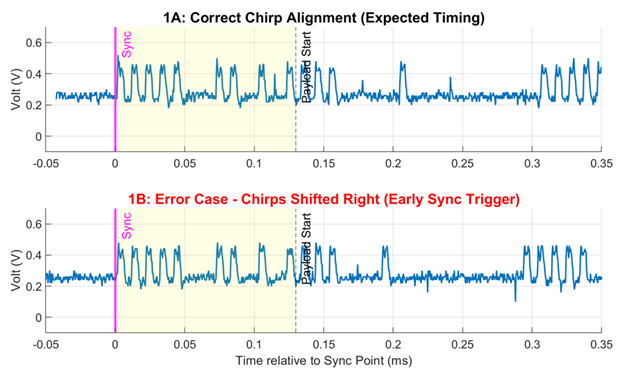
    I am using a timer on the MCU to generate the trigger signal. When the trigger is sent, the LMX is expected to generate a frequency ramp from 12 GHz to 12.125 GHz. On the receiver side, I observe a sine wave because I am using an envelope detector to downconvert the signal.

    I have attached the received signal for reference. As shown, the ramp around 0.2 ms appears to be triggered earlier than expected.

  • Hi Yu-Cheng,

    Is below something you want to implement? 

    Please note, your required linear ramp range is125MHz, this may or may not be possible with LMX2595, this range is not ensured by the device and may vary from part to part. To get linear ramp, Threshold must be set to larger than the ramp range, otherwise there will be calibration during the ramp.

  • Hi Noel, 

    Yes, that's actually what I want to implement on LMX2595EVM. 

    If 125 MHz ramp is not ensured by the device and may vary from part to part, what's the ensured range by this device? Thank you.

  • Hi YuCheng,

    The linear ramp is not ensured because we did not test this item in product.

    in general, if the ramp frequency is in the middle of a VCO core, it is more likely that the linear range is repeatable from part to part and over temperature. The linear range could be up to 100MHz. However, if the ramp frequency falls into the boundary of two adjacent VCO core, the linear range is hard to tell. For example, if we use VCO4 to ramp from 12GHz to 12.1GHz. The PLL may lose lock when the ramp reach 12.05GHz because that may be the max. frequency that VCO4 can support.

  • Thanks for the explanation.

    I would like to confirm my understanding of the issue.

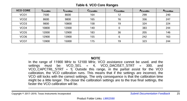
    From the datasheet note, it seems that the 11900–12100 MHz region has special calibration constraints. Does that mean this frequency region is the main reason why a ramp around 12 GHz is difficult to guarantee?

    If so, would shifting the chirp fully outside that region be a practical workaround? For example:

    • 11.7 GHz to 11.825 GHz, or
    • 12.125 GHz to 12.25 GHz

    Would these ranges be more likely to provide reliable PLL lock and repeatable ramp behavior?

    Also, since Table 6 shows that VCO5 covers 12 GHz to 12.9 GHz, I am wondering whether using VCO5 directly for a 12–12.125 GHz ramp is possible, or whether there is an internal limitation that still forces the device toward VCO4-related behavior in this region.

  • Hi YuCheng,

    The note applies to partial assist calibration, there is no issue with no-assist calibration.

    However, 11.9G to 12.1GHz fall into the boundary of two VCO core, this region is not ideal for linear ramp.

    The proposed new frequency ranges are better, pretty sure that they are away from the boundary.

    12GHz is in the boundary of VCO4 and VCO5, if we force the device to use VCO5, part to part and temperature variation may affect the operation at lower frequencies (close to 12GHz) of the ramp.