Part Number: LMK04828BEVM
Other Parts Discussed in Thread: LMX2594, LMK04828, LMK04832
Hi Team
As shown in the attached block diagram “SETUP-BD”, we are using LMK04828B and LMX2594 on our custom board to provide all RF reference clocks and the SYSREF clock to the RFSoC 49DR device.
As shown in the block diagram, we are testing multi-SoC synchronization for the DAC channels generated from two RFSoC 49DR devices.
We are using an external clock source through a splitter to provide synchronized clocks to LMK CLKIN0, in order to lock both LMK04828B devices with in-phase external clocks. Additionally, we are using a trigger to generate the DAC outputs at the same time.
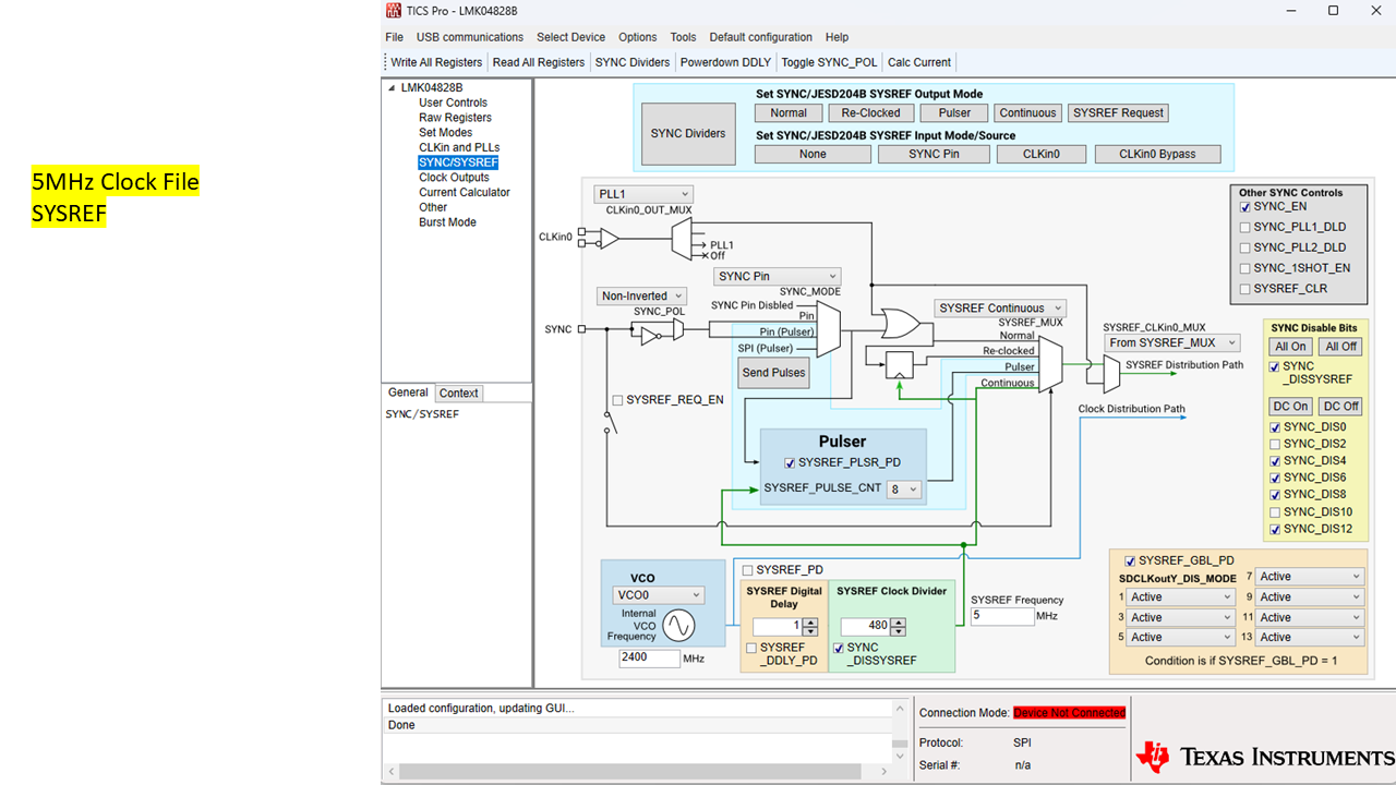
We are able to synchronize both RFSoC DAC outputs when using an external 5 MHz clock source. Both DAC outputs are in phase. I have attached the LMK04828 configuration files used for this test case (“5MHz-LMK” and “5MHz-LMK-SYSREF”).
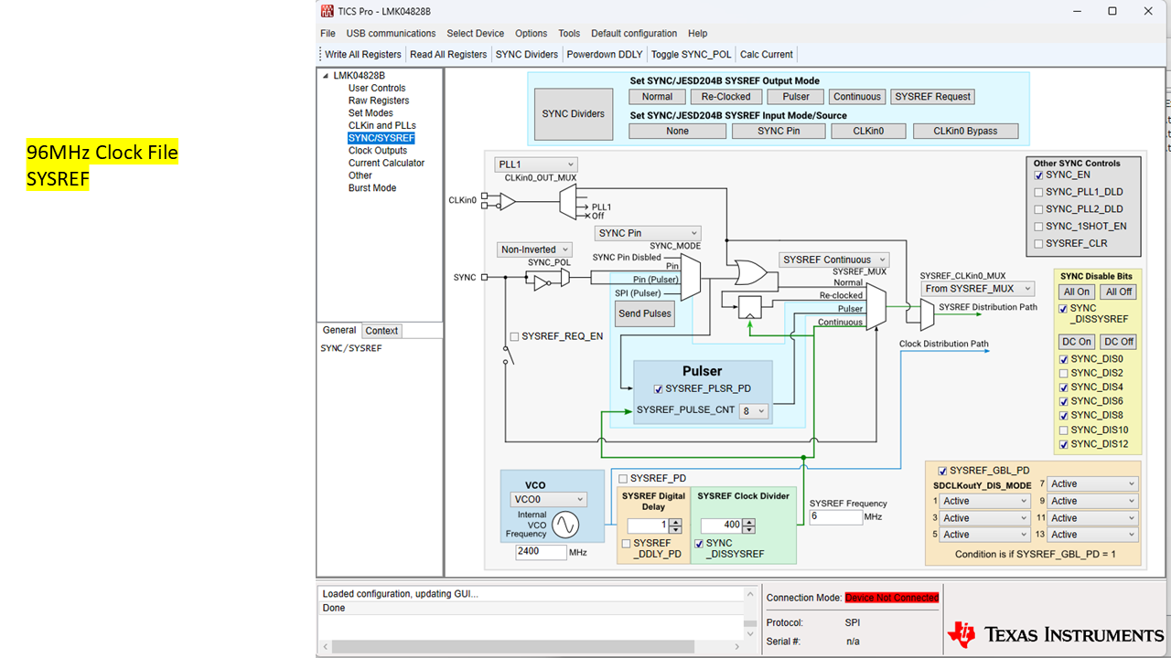
For some applications, we need to use an external 96 MHz clock instead of 5 MHz to synchronize the LMK04828B. I modified the existing 5 MHz CLKIN0-based clock configuration to 96 MHz, as shown in the attached snapshots (“96MHz-LMK” and “96MHz-LMK-SYNC”). However, when using the external 96 MHz clock, even though PLL1 and PLL2 of the LMK04828B are locked, we observe a phase difference between the DAC outputs.
Upon further investigation, we found that there is some delay in DAC generation when using the 96 MHz clock configuration.
Initially, I used a PLL1 R divider value of 96 to match a SYSREF clock of 5 MHz, and we observed a larger phase difference compared to the attached 96 MHz clock configuration (where a PLL1 R divider value of 16 is used).
My questions are:
- What procedures should be followed to synchronize the LMK04828B using an external 96 MHz clock?
- Do I need to provide an additional trigger to the SYNC pin of the LMK when using a 96 MHz external clock?
- Do you have any application notes that explain multi-LMK04828B synchronization?