Part Number: CDCLVP1102
Dear Sir/Madam,
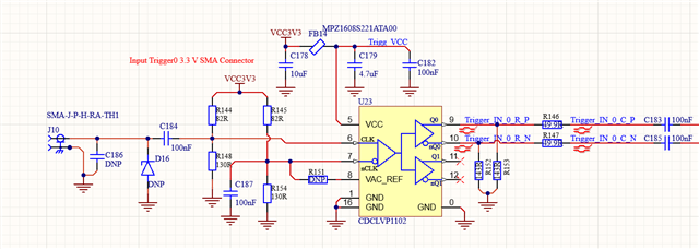
in our project we used CDCLVP1102 as input trigger interface to the FPGA. As the chip is LVPCEL it is powered with 3.3V and the FPGA bank is powered with 1.8v. According the FPGA documents , the LVDS IVDiff is minimum 100mv and nominal 350 mv. The output of the CDCLVP1102 is pulled down to GND with a 150 ohm resistor and there is a series resistors 70 ohm to the fpga to reduce the swing from 600 mv to 350mv according to https://e2e.ti.com/support/clock-timing-group/clock-and-timing/f/clock-timing-forum/870502/cdclvp1102-lvpecl-to-lvds?tisearch=e2e-sitesearch&keymatch=CDCLVP1102#
there are also two ac-coupling 100nf capacitors to block dc bias. The FPGA inside DC bias and 100 ohm termination is activated.
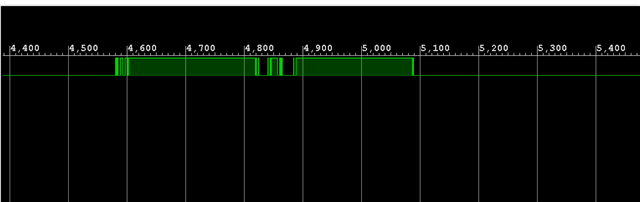
when there is no signal in the input of the chip ( it is ac coupled input) the output of the chip is noisy and it fluctuates more than 100 mv that is why in the FPGA a random pulse is generated .
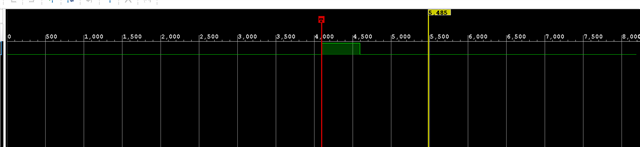
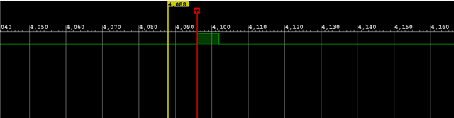
when I connect a pulse to the input, at the FPGA pins I measure the pulse but still the IBUFDS in the FPGA generates a random pulse. ( the pulse frequency is very low )
when the input of the chip is several KHz square wave, the result is the same.
when the input of the chip is above 1 MHz square wave, I receive a clean sqaure wave with the same frequency.
I would like to ask why the output of the chip fluctuates more than 100 mv when there is no signal or less than 1 MHZ singnal. Is there anything which we have overlooked in our design?
I would like to thank you for your help and support in advance.
many regards,
Hamed Sotoudi