This thread has been locked.

If you have a related question, please click the "Ask a related question" button in the top right corner. The newly created question will be automatically linked to this question.

CDC6C: 2.4GHz Emissions Causing Wi-Fi & BT Desense

Part Number: CDC6C

Hello, 

We have recently replaced our critical networking oscillators with the CDC6CE025000ADLFR. This has helped with our unit to unit clock accurancy and jitter. However, our system also has Wi-Fi and BT radios. We recently got our TIS report back and it showed a 30dB desense when measuring TIS over the air vs directly connected to the RF port. 

I am seeing very strong emissions at 2.5GHz and a stong comb spectrum with my near field pobe. I am actually picking up the 2.5GHz oscillator with my probe 3' from the PCBA. I do not see the emissions in the traces leading into or out of the device. This leads me to believe they are coming from the IC itself. 

My power is locally decoupled and directly connected to a large internal power plane. I will look at isolating the power for the IC locally with a ferrite and cap filter. But I do not expect this to make a significant differnce. 

Do you have any insight into the emissions profile for this oscillator at 2.4-2.5GHz? Any debig recommendations? 

Thank you, 

Adam
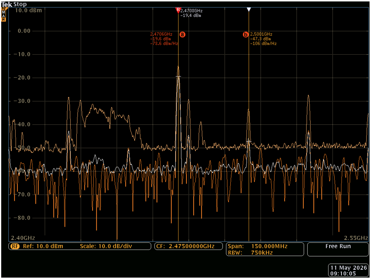
image.png

  • Hi Adam, 

    The CDC6C oscillator has an internal tunable resonator in the 2.5GHz range, which then gets divided down to provide the final output clock frequency. I assume this is what you're observing but I'm surprised to see so much power in this band. The resonator has an extremely small feature size so we generally don't see it contribute much EMI, for example in our CISPR-25 EMI report the peak ~2.5GHz noise was in the range of 30dBuV/m. You could refer to the full EMI report here for more details: https://www.ti.com/lit/an/snaa438a/snaa438a.pdf 

    Are you supplying the part with 1.8V, 2.5V, or 3.3V? And do you only see a concerning level of noise in this 2.5GHz region? 

  • Hello Connor, 

    Note that I am using a 30dB preamp with my near field probe, and we have passed EMI testing at that frequency. However, I am currently just looking into a desense issue on the radio. Since we are in a metal chassis with a cut out where the antenna is placed through we could have a very high Q reverb chamber for the BAW to resonate in. 

    We do not see similar desense issues at 5GHz. 

    We are supplying 3.3V and using a 3.3V component. 

    The layout is fairly basic. The highlighted components are the bypass cap and oscillator. This is a 6-layer design with contiguous ground on 2 and 5, and power planes on layer 4. 


    If I disable the clock (pull pin 1 low) I see the CW spurs in the above spectrum disappear. There is a little residual 2.5GHz from something in my environment but the 2.47GHz spur is gone. 

    Placing my processor in reset also does not have any affect on the emissions. 

    I currently have the option to populate traditional XTALs in the design and have asked for the test to be completed again with those populated and the oscillators disconnected and in reset. I do not have a timeline on this testing. 

  • Hi Adam, 

    Unfortunately we don't have other data available on the emission profile for CDC6C aside from the CISPR-25 report that I sent in my previous reply. Just to make sure I'm understanding correctly - the CDC6C is clocking the processor, and when the processor is in reset there's no affect on emissions. When the CDC6C clock is disabled, the emissions completely disappear. Overall this points to the CDC6C being the original source of the 2.5GHz emissions and it's not likely to be anything downstream generating this noise. Does this sound accurate?

    I'm not sure if this is worth trying but would it be possible to depopulate the component connecting the oscillator output to the XIN input (I believe this is C12)? I'm hoping that this could provide some more information to confirm if the 2.5GHz noise is intrinsic to the oscillator itself, or if it could somehow be coupling to the output and radiating through the output traces. Aside from that I think your strategy of testing with a passive xtal could also provide more information on where the noise originates from.  

  • Hi Adam, Conor

    If board from https://www.ti.com/lit/an/snaa438a/snaa438a.pdf works OK then I would try something like that with 2-4 additional 0402 or smaller X7R MLCC decoupling caps.

    I would also consider using IC in smaller package like DLX or DLY.

    Regards,

    Grzegorz

  • The state behavior is correct. 

    We currently have XTAL testing in process. We expect results tomorrow. 

  • The differences in package size, operating voltage, and local bypassing are noted. One of the two oscillators we can operate at 1.8V. 

    We will revise the layout. Unfortunately the EVK has a very different layout and bypassing scheme than the CISPR test board. It would be good to know if there were specific emissions that caused the CISPR tests to be run on a different PCBA. If it was specifically due to emissions in the 2.4-2.5G band that would give me confidence in keeping the component in our design for the next build (revised layout, smaller package). 

  • Hi Adam, 

    Regarding the layout differences between the CISPR test board and the EVM, we didn't necessarily make these changes to target specific emissions. The intention was to minimize the output trace length and reduce the impact of the output trace in the EMI results. For this compliance testing we typically just want to validate the intrinsic noise of the oscillator. The bypass caps were optimized to reduce the oscillator switching noise from feeding back into the power supply and radiating throughout the power plane. I believe we chose caps which had very low impedance at the switching frequency (25MHz), as well as the equivalent frequency of the rise time (1 / 1.47ns = 680MHZ for slow mode 2 variants). 

    Did you see any improvement after testing with the xtal?  

  • Hello Connor, 

    Yes we did see an improvement. We saw a 24.09dB improvement at CH1 (2412 MHz) and 34.24dB improvement at CH13 (2472 MHz). 

    I am going to leave the oscillator footprint on the PCBA for the next build, but change to the DLX package (DLY out of stock), add a capacitor bank targeting 2-3GHz, and a ferrite bead isolating the oscillator from the power net. I have found a few Murata ferrites that specifically work in the 2.4GHz band where SRF is not an issue. 

  • Thanks for the update here, hopefully the layout optimizations will solve this issue on the next build. I'll go ahead and mark this thread as resolved but feel free to create a new thread if you have any other questions. 

  • I also just looked at the potential for noise to be generated strictly by the rise time of the output driver. 

    Test:
    1. Use an E field probe to monitor emissions on output trace and H field probe to monitor emissions above IC. 

    2. DNP series output component.  Float the output. 

    3. Repeat measurements with E and H field probes. 

    Observations:

    The stock unit showed significant emissions on the output trace when using the E field probe.

    After modification, no emissions were shown on the E field probe and the spectral lines did not shift when viewed with the H field probe. Magnitude viewed with the H field probe was relatively unchanged, but the measurement error is massive here. 

    If the emissions source were rise time harmonics the change in output capacitance should have shifted the emissions spectrum. The data sheet shows a significant shift between just 2pF of loading and 5pF. I am assuming that I removed a few pF of loading at the very least.