CDCE6214: CDCE6124 syntonized clock servo

Part Number: CDCE6214
Other Parts Discussed in Thread: , ADS1235

Hi TI team
We're looking to use the CDCE6124 in a clock servo application where we use it to syntonize all local clocks (ADC @ 7.3728MHz , MCU @24 MHz, and MAC/PHY @ 25MHz) to a network timereference (gPTP protocol). 

Comparing local counters with sync messages the protocol outputs an error estimated to be within 150ppm with sync rate every 125ms. Step size sufficient around 1ppm

Is the device suitable for this application?
- Can the CDCE6214 continously adjust all frequencies in positive and negative direction, starting from the mentioned nominal frequencies
- Is the device suitable to avoid clock glitches when applying change?
- REFSEL to low, with an XTAL input as SECREF as a correct choice, no PRIREF?
- Based on the example 7.2.3 in the data sheet , how is the frequency best steered in this servo loop? DCO mode on,  then with evey correction signal,  FREQ_INC_DEC_DELTA gets applied to the numerator, correct? What is the role of the DCO output divider, as exposed in TICSPro?
- Any difference between the product versions, regarding registers and controlling the servo?

Somewhat related post: (1) CDCE6214-Q1: Output Clock Pull Range - Clock & timing forum - Clock & timing - TI E2E support forums :

  • Hi Tobias,

    We're currently looking into your query, we will get back to you within the next few days. 

    Best,

    Jaryd

  • Hi Tobias,

    Apologies for the delay. To be sure I'm responding to all your questions, I'll list my answers below:

    Is the device suitable for this application?
    • Just to clarify your question, are you saying you need to make DCO adjustments with a range of +/-150ppm every 125ms?
    Can the CDCE6214 continously adjust all frequencies in positive and negative direction, starting from the mentioned nominal frequencies
    • The CDCE6214 can adjust frequencies in DCO mode with a step size of 10ppb or less.
    • If you need to reset the adjusted frequencies back to the original value, the only way to do this is to do a software reset on R0[2] (with DCO enable bit set to 0), which will disrupt output clocks. Otherwise you have to "manually" reset it by incrementing/decrementing the frequency back step by step via I2C.
    Is the device suitable to avoid clock glitches when applying change?
    • Each output channel divider has glitchless switching and synchronization capabilities, this also applies when in DCO mode.
    REFSEL to low, with an XTAL input as SECREF as a correct choice, no PRIREF?
    • This is correct, pulling REFSEL low will select the XTAL input on SECREF.
    how is the frequency best steered in this servo loop? DCO mode on,  then with evey correction signal,  FREQ_INC_DEC_DELTA gets applied to the numerator, correct? What is the role of the DCO output divider, as exposed in TICSPro?
    • Your interpretation looks correct. Each rising edge of FREQ_INC/FREQ_DEC increases/decreases the output frequency by the step size set for FREQ_INC_DEC_DELTA.
    • The role of the DCO output divider is to enable fine frequency margining. With this enabled you can get step sizes of 10ppb or less.

    Any difference between the product versions, regarding registers and controlling the servo?
    • Which products versions are you asking about? There is no difference in registers between the CDCE6214, CDCE6214-Q1, and CDCE-Q1TM, if this is what you're referring to. The Q1TM does not have I2C capabilities, and the Q1 has been qualified for automotive applications.
    can I 24MHz Xtal be used as SECREF?
    • Yes the CDCE6214 can accept a 24MHz XTAL as SECREF.

    Best,
    Jaryd

  • Hi Jaryd, 

    Thanks a lot for your answers. 

    To clarify the range: The 150ppm would be the total range, where we think we need to steer,  an adjustment of the control loop would probably be much lower, like +/-  1 to10ppm.

    Second question was just to confirm the product versions are identical.

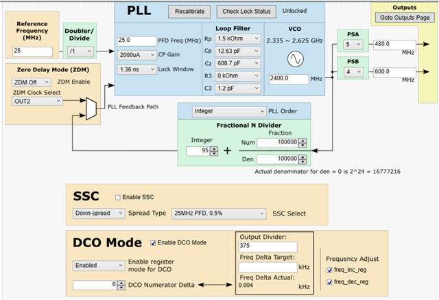
    Based on my understanding, I would then configure the device as in the picture below, this would give a sub-ppm step size on the ADC clock.

    1) Follow up question regarding the DCO Mode fields in the black rectangle: Output divider and Freq Delta Target are not really configuration fields on the device, they are just to there for help the calculation of what the frequency change will be, correct?

    2) It seems that there is no factory configuration to pass a 24MHz XTAL reference to an output at startup that can later be adjusted through the DCO, correct? (We have to write a configuration to eeprom first) 


  • Hi Tobias, 

    Thank you for clarifying! We're currently investigating internally how to properly setup and configure DCO mode, we have a high-level description of DCO mode in the datasheet that you can refer to in the meantime. We will get back to you soon regarding this. 

    1) The output divider and freq delta target are windows that are populated once the DCO registers are set, I'll look more into this as well. 

    2) We unfortunately don't have a factory configuration with a 24MHz XTAL with DCO mode on, so this would need to be configured based on your use case. 

    Best,
    Jaryd

  • Hi Tobias,

    Just wanted to get back to you regarding the behavior of DCO mode for the CDCE6214. I ran a setup in our lab with the same TICS Pro configuration and these are my findings:

    • The Output Divider and Freq Delta Target fields on TICS Pro are for calculating the DCO numerator delta, which will give you the incremental step size on each rising edge
      • The Output Divider value is the VCO frequency divided by the output frequency. So if your VCO freq = 2400MHz and your output is 24MHz, this should be set to 100.
    • This increment can go in the positive or negative direction depending on whether freq_inc_reg or freq_dec_reg is changed
    • The output frequency will increment/decrement in DCO mode during a 1 --> 0 transition of freq_inc_reg/freq_dec_reg, and the step size can be configured using your desired frequency delta target (in your case this would be ±1-10ppm)
    • The PLL Order of the N-divider should be set to "Frac Order 3" because DCO mode works by adjusting the numerator of the sigma-delta modulator

    Let us know if you have any further issues with the setup of DCO mode for the CDCE6214, and if there are specific jitter requirements you are looking for, as I saw this was affected when incrementing/decrementing the output frequency.

    Best,
    Jaryd

  • Hi, many thanks for your setup.

    Jitter is indeed a factor. Is there a way you can qualify what you observed in an RMS value? from your datasheet i get a maximum of 4ps in fractional mode. 
    I believe this is fine. 

    Reasoning (if I am correct) : 
    The ADS1235  converter is Delta Sigma, discrete time, switch cap sample and hold, which I understand are less sensitive to jitter. 


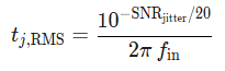
    Using 


    solving


    for RMS jitter and plucking in the quantization noise limit  for SNR:


    We get values that are somewhere around the 10ths of ns worst case for ENOBs from the datasheet and playing with OSR...

  • Hi Tobias,

    I'm confirming your understanding with our design team, as they should have more detailed/accurate information on what you can expect in terms of RMS jitter when incrementing/decrementing the output frequency in DCO mode. I'll get back to you once they've completed their analysis. 

    Best,
    Jaryd

  • Hi Tobias, 

    I have confirmed with our design team that you should be able to observe an RMS jitter value below 4ps depending on the charge pump gain and divider values you have set in the loop filter design. Decreasing the charge pump gain will make the device more resilient to the effects of incremental output frequency adjustments via DCO mode. Increasing the N-divider value (while maintaining the same VCO frequency by adjusting the reference clock divider) will also have the same effect. 

    I observed an fairly high RMS jitter value in DCO mode when I initially tested the device in my setup, but after adjusting the charge pump gain I was able to see jitter values of 4ps and lower. We also have a tool called PLLatinum Sim that can help you simulate the loop filter values to ensure the filter is stable. There is no profile specifically for the CDCE6214, but using the custom profile and inputting your loop filter component values should work as well. 

    Best,
    Jaryd

  • Thank you very much, we'll try it out, once we have the dev kit

  • Hi Jaryd, would it be possible to share your register configuration file as a reference point?

  • Hi Tobias,

    Here is the register dump for the config I used in my setup: HexRegisterValues_dco.txt
    Here is the TICS Pro file as well: CDCE6214_dco.tcs

    I used PRIREF to test this configuration since the EVM I was using did not have an onboard XTAL, so you may have to update this on your end if you're using SECREF. Also this config is from before I changed the loop filter/CP gain settings to reduce the DCO mode effect, but it might be best to experiment with these values to achieve the RMS jitter you are looking for. 

    Best,
    Jaryd

  • Thank you very much, that worked. 

    I would now like to examine the clock behavior after we give a freq_inc signal to the CDCE6214.

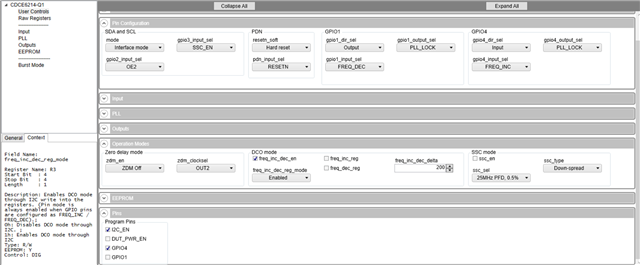
    With your evaluation kit I can't seem to get the hardware signal input on GPIO4 to trigger a increment for the DCO. Register mode triggering works. What am I missing? Here is the configuration: 

    I measure 1.8V on the GPIO4 floating, that's probably an internal pull-up. I then pull it low and release it with the jumper. The idea is to use this as the trigger for the oscilloscope looking at all the signals.

  • Hi Tobias,

    It seems like you are performing the increment correctly with the GPIO pins; I will test this in our lab and get back to you shortly. 

    Best,
    Jaryd

  • Hi Tobias,

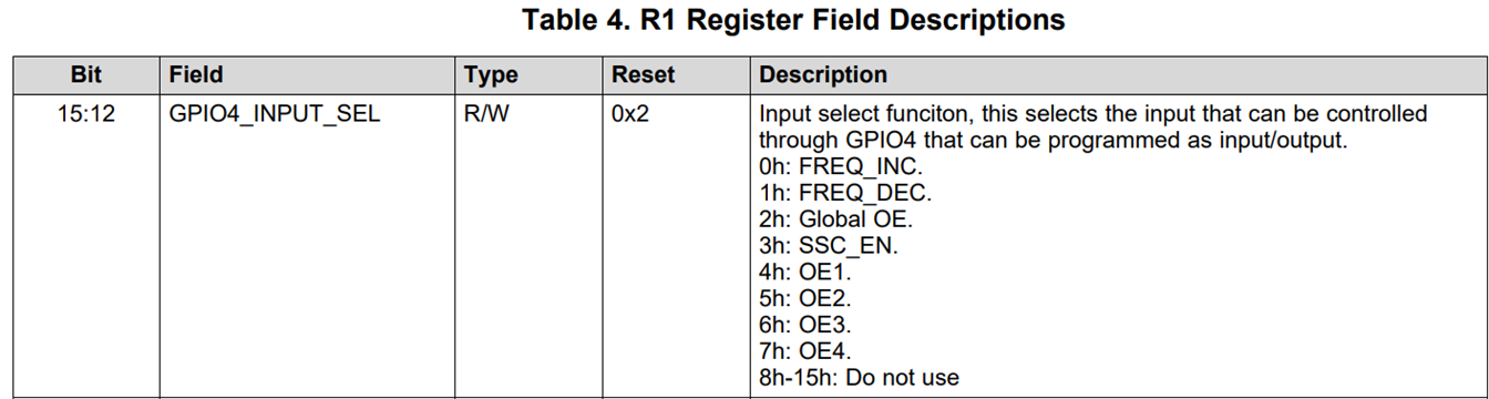
    In the register dump I sent you, I had not configured the GPIO pins properly since I was incrementing/decrementing using I2C, so when you write to EEPROM the GPIOs will not be properly configured as FREQ_INC/FREQ_DEC in pin mode. If you are looking to use GPIO4 as your increment or decrement, you can update this raw register according to the CDCE6214-Q1 register map while connected via I2C, write the registers to EEPROM, then boot in pin mode to use the GPIOs.


    Based on the register map and the register dump I sent you, GPIO2 should be configured as FREQ_DEC as well, so it may be worth it to check whether this GPIO will decrement the output as well. 

    Best,
    Jaryd

  • Thanks a lot, but unfortunately I still didn't work. 

    I configured the pins as Input, wit DEC and INC functionality, activated the pins. Had HW_SW_CTRL floating, commited everything to eeprom. Started the device from EEPROM page 0, by setting HW_SW_CTRL low. Then, set the jumper on GPIO4 to pull down, and connected and released, to VDDREF, verified with a voltmeter. The cdce6214 did not change the frequency. 

    Could you send me a working configuration from your end. Attached is my configuration...

    Many thanks!


    CDCE6214_dco_mt.tcs


  • Hi Tobias,

    It seems like your methodology is once again correct; I'll investigating internally why the DCO mode configuration in pin mode is not properly incrementing the output and I'll get back to you as soon as possible. 

    Best,
    Jaryd

  • Hi Tobias,

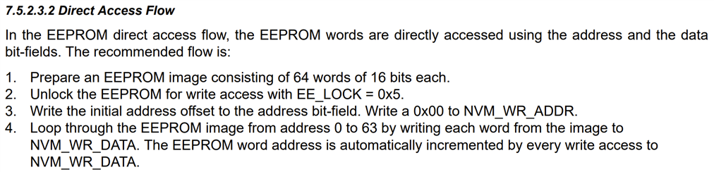
    According to the CDCE6214 register map, the device mode register can only be written to EEPROM using the direct access method.

    The process on how to write using the direct access method is listed in the datasheet, I've attached the section below for convenience.

    Here is the step-by-step process to program the EEPROM in pin mode that I performed:

    1. Configure device in fallback mode (SDA/SCL pulled up, HW_SW_CTRL floating)
    2. Load TICS Pro configuration (.tcs)
    3. Set EE_LOCK = 0x5
    4. Set NVM_WR_ADDR = 0x00
    5. Set mode (R0[0]) to 0x1
    6. Configure other device settings as desired
    7. EEPROM >> Register to EEPROM
    8. EEPROM >> Read EEPROM to file
    9. Open EEPROM image in notepad and increment the hex AND decimal values of line 16 (page 0) or line 40 (page 1) by 1
    10. Write file to EEPROM with the edited .hxt file
      1. NVM_WR_ADDR should now read 63
      2. There may be a CRCERR, but it should still write to EEPROM
    11. Boot the device into pin mode - float GPIO2/3, set HW_SW_CTRL low (page 0) or high (page 1)
    12. Device should now be in pin mode with the selected page and proper EEPROM configuration

    With these steps I was able to observe OUT1's output frequency increment when I pulled GPIO4 down. The increment step itself was unstable and inaccurate, but this is likely because I used jumper pins to pull GPIO4 low since this method introduces lots of ringing to the pin. For more accurate increment/decrement, it is best to send the FREQ_INC or FREQ_DEC signal through an external microcontroller or ASIC.

    Here is the EEPROM file that worked on my end: cdce6214_dco.hxt

    To write this to your device, you can use steps 10-12 in the above process. I've configured the EEPROM image for the following settings, but if you'd like to change them, the steps above should work.

    Best,
    Jaryd

  • Thanks Jaryd, this approach worked