LMK04832: LMK04832 sysref phase alignment not working

Part Number: LMK04832
Other Parts Discussed in Thread: LMK04828,

We have two LMK04832 devices and would like to synchronize the outputs.
 
Both devices use OSC input that runs at 100MHz. These two are fairly aligned.
We are driving sync input of each device from an FPGA and we have verified that they are fairly aligned.We are sending 10ns pulses as sync input from the FPGA.
 
We are following the following procedure:
  1. Write 0x51 to register 0x143. This sets SYNC_EN, SYNC_1SHOT_EN, and sets SYNC_MODE to use sync pin.
  2. Write 0x00 to register 0x139 . This sets SYSREF_MUX to Normal (use sync pin)
  3. Write 0x00 to register 0x144. This enables sync on sysref and output clocks
  4. Send a sync pulse from the FPGA
  5. Write 0xFF to register 0x144. This disables sync on sysref and output clocks
  6. Write 0x11 to register 0x143. We learned that SYNC_1SHOT_EN needs to be disabled, and not sure why.
  7. Write 0x03 to register 0x139. This sets SYSREF_MUX to continuous so we get sysref on output pins
 
We have done some variations of the above, for example, not enabling SYNC_1SHOT_EN. We have also tried using the CLKin0 path.
 
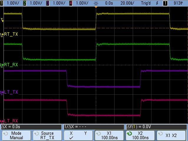
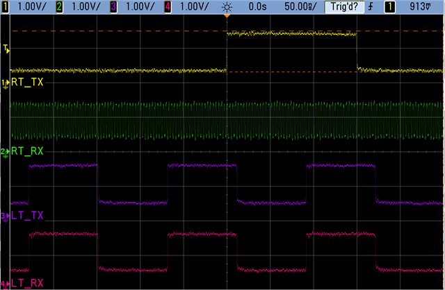
The way we are debugging is that we are looking at the sysref from the two devices with a scope. There is a given skew between the two since they are not synchronized yet.
Our expectation is that if we go through the sync procedure above for only one device, and we move the sync pulse by 10ns/20ns/etc., the skew between the two sysref signals from two chips adjusts by the same delay amount. We are not seeing that. The relative skew between sysref output of the two devices remains the same.
 
We are fairly confident that the devices are receiving the sync pulse. If we don't enable the 1shot bit and generate the sync pulse (step 4 of the above procedure), we can see the pulse reflected in the syncref output of the device.

Baseline configuration attached:
lmk04832_pl312_sys6p25_armed_v2.tcs
  • First, make sure that SYSREF_DDLY ≥ 8. SYSREF_DDLY=0 is a reserved value and performing the SYNC procedure with SYSREF_DDLY=0 may not produce predictable behavior.

    Second, make sure that you are also asserting SYSREF_CLR=1 at some point during the procedure before the SYNC pulse is sent. You could modify step 1 to write 0xD1 to 0x143, and this would be sufficient. This clears the SYSREF local delays and ensures they are primed for operation.

    There is a single one-shot timer located after the SYSREF_MUX. The SYSREF_MUX and the SYSREF distribution path are used by both the divider reset process (SYNC) and the SYSREF divider distribution. If the one-shot is enabled when you switch the SYSREF_MUX to continuous, you get the output of the one-shot on the output pins every time the SYSREF divider rising edge triggers it. 

    If the SYNC procedure is performed without using SYNC_1SHOT_EN, the dividers are held in reset until a logic low condition is latched by the clock distribution path (i.e. when the SYNC pulse from the FPGA ends). This could impact your results if the SYNC pulse falling edge is always at the same phase offset relative to the SYSREF divider, regardless of rising edge delay, but this doesn't explain why the issue is observed with the one-shot enabled as well.

    First, try repeating the procedure with the two suggested amendments (SYSREF_DDLY ≥ 8, include SYSREF_CLR=1 by modifying step 1 to write 0xD1 to 0x143). If you still observe problems, let us know, and we'll investigate further.

  • Hello Derek, thank you for your speedy response.
    I tried what you suggested, writing 0xD1 to 0x143 in step 1.
    I also set SYSREF_DDLY to 8:
    Wrote 0x00 to 0x13C
    Wrote 0x08 to 0x13D

    The behavior did not change. I ran the sync procedure on only one chip. Even after the first attempt, the relative position of sysref output from the two chips did not change. Of course we lose sysref during the procedure, but when it comes back, it is in the same relative position as before. I moved the sync pulse and confirmed that it makes no difference, as if the sync procedure is completely ignored.

  • As a sanity check, can you try modifying the local digital delay field for the SYSREF being measured (SCLKx_y_DDLY) and confirming that the delay changes by the equivalent number of VCO cycles? For instance, if you have 2 cycles set, and you modify the digital delay to 6 cycles, we would expect to see one nanosecond of phase shift (4 / 2500MHz). This field can be modified with the outputs running.

    Another sanity check: when you send the SYNC pulse, do you see the clock outputs temporarily held in a static state for the duration of the SYNC event (plus several VCO cycles as determined by DCLKx_y_DDLY)? This helps confirm that any dividers are being reset.

    A third sanity check: instead of delivering a SYNC pulse via FPGA GPIO, can you toggle the SYNC_POL bit (0x143[5]) to 1 then to 0 in step 4 via SPI by writing 0xF1, then 0xD1, to 0x143? The SPI timing is likely asynchronous relative to the other operations, and for a single device synchronization the procedure could be repeated with no deterministic relationship to the SYSREF, forcing a randomization of the resulting SYSREF divider phase. If even this is producing the same SYSREF phase, I will be quite surprised.

    You describe moving the SYNC pulse by 10ns/20ns/etc, for only one device. What does it mean to move the SYNC pulse by 10ns for only one device? Is there some system GCD frequency acting as a repeatable t=0ns reference for the SYNC experiments? Assuming yes, is it possible the reference frame is moving with the SYNC pulse in such a way that the resulting phase shift is being cancelled out? I don't see anything wrong with your procedure, and you describe behavior that sounds like the device is being programmed correctly; the remaining explanations suggest the timing of the external SYNC pulse is responsible. The third sanity check should investigate this possibility, provided the SPI timing relationship is not phase-locked to the SYSREF.

  • I am seeing something strange with SCLK8_9_DDLY (register 0x126) that I can't explain. In TICS pro the value shows as 2. When register hex values are exported the value shows as 1.
    If I set this register to any value between 0 and 4, sysref signal does not move. If I set it to any value between 8 and 15, sysref moves by 3.2 ns (8 x 400ps).

    As a sanity check I looked at the SPI signals with a scope. They look good. Clock is running at 4MHz and when I wrote to 0x126, SCLK and MOSI made sense.
    Datasheet description for this register seem to indicate it needs to have a minimum value of 8, but POR default is 0.
    Maybe you can shed some light on this.

    I noticed we are exporting the hex values from TICS Pro, and initializing the registers based on that, before we do the resync processing. It seems to me like we would be trying to write over some read-only registers, like device ID. Is this OK?

    The second sanity check: I don't see the clock output freeze when sync pulse is sent.

    The third sanity check: I had already done this and verified it again just now. toggling SYNC_POL instead of sending a sync pulse in my resync procedure does move sysref with respect to the other LMK device. As expected, the phase relation between the two LMK devices moves randomly as SPI sync is happening at a random time. The 312.5 MHz clock also seems to move.

    Is this telling us something about 10 ns pulse width being a problem? As indicated before, when 1shot is not set, I can see the pulse propagate through to sysref output, so I believe the device is receiving the pulse.

    Even in the SPI resync method, where we see the sysref actually move, the clock output does not seem to freeze. I am not 100% confident about this as I don't use this feature of the scope that often.

    I am 100% sure when I attempt resync with the 10ns pulse: the clock keeps running normally around the time the pulse is asserted.

    Let me go over how I am monitoring all of this, and hopefully this will answer your question.

    Both LMK devices are receiving the same 100MHz osc input that are aligned. When I initialize both devices, the sysref output of both devices maintain a fix skew. So, when I trigger on rising edge of LMK 1 sysref output, I can see LMK 2 sysref output at a random phase and not moving.

    After this point I don't touch any of the LMK 1 registers and sysref of that device becomes my reference point.

    When I perform the resync procedure on LMK2 with 10 ns pulse, I can see LMK 2 sysref output get disrupted, but after the procedure is done, it keeps the same phase with LMK 1 as before the procedure was done.

    There is another signal synchronous to the 100MHz osc input that FPGA uses a reference. If you picture the two LMK sysref outputs on a scope, I can move the 10ns pulse around anywhere relative to the two waveforms. I expect that if resync worked, the relative phase of the two sysref to change based on the sync pulse being asserted in a different position. However, regardless of where the pulse is positioned, the relative phase between the two sysref remains the same. Keep in mind that LMK1 registers are untouched, and FPGA is not capable of moving the other reference signal that allows it to move the sync pulse around.

  • Correction to my previous post where I said:
    "If I set it to any value between 8 and 15"

    I meant to say:
    "If I set it to any value between 5 and 15"

  • I increased the sync pulse to 150ns. Instead of writing 0xD1 to 0x143 in step 1, if I write 0x11, I can see the pulse flow through to sysref output. I did this just to confirm that the chip is seeing the sync pulse.

    The third trace from the top is the pulse going to the chip, and the fourth one is sysref out of the chip (the top two are sysref from LMK1 chip that I use as a reference). It looks like there is a bout a 16ns delay for the pulse to go through the chip.

    Why toggling SYNC_POL causes a sync but a 150 ns pulse does not? SYNC_POL is a lot longer as our SPI accesses are very slow. Since we are setting the 1shot bit, only the rising edge should matter.

  • This is just a visual of what I am seeing. The top two are the same sysef signals from LMK1. The bottom two are from LMK2. I can assert the sync (now 150ns wide) anywhere in this window, and the relative position of the two does not change:

  • And now I do a sync with SYNC_POL instead, and the relative position of the two move. If I keep doing this, the two randomly move with respect to each other because SPI accesses happen at random time.

  • The behavior you describe is exceptionally strange. It is difficult to imagine how the SCLKX_Y_DDLY write is not producing the expected behavior.

    Are you certain that the device on both of your boards is LMK04832, and one or both are not something with the same package and pinout but a slightly different register set (such as LMK04828)? SCLKX_Y_DDLY is offset by 0x02 from LMK04828 to LMK04832, which could potentially explain the observed behavior; but I am skeptical you would see anything out of the SYSREF since one of the bits being written in the LMK04832 registers -> LMK04828 device translation should be shutting down the SYSREF on odd-numbered outputs. I'm also thinking you'd notice if you configured CLKOUT8 and CLKOUT9 to be SYSREF, but CLKOUT8 did not produce a SYSREF on one of your devices (LMK04828 does not have a path for SYSREF to CLKOUT8).

    footnote: SYSREF_DDLY needs a minimum of 8, SCLKX_Y_DDLY values are from 0x00 to 0x0A (bypass to 11 cycles). The datasheet has a mistake, we're working on updating that.

  • I verified that ID_PROD (registers 0x4 and 0x5) and ID_MASKREF (register 0x6) match LMK04832 datasheet.
    I repeated the experiment of setting register 0x126 (SCLK8_9_DDLY) from 0x0 to 0xa, and verified the settings by reading back the register.
    I only get a jump when value changes from 0x04 to 0x5. Is there any other register setting that could explain this behavior?
    I increased the sync pulse to 640 uS (no good reason, just wondering why toggling SYNC_POL that is slow works). No change in behavior.

  • Apologies, I will be somewhat delayed in my responses moving forward due to conference attendance.

    The local delays are equivalent to a chain of D flip-flops clocked by the clock distribution path, and a mux selecting the delay tap. Asserting the SYSREF_CLR bit (0x143[7]) for 15 VCO cycles should be sufficient to completely clear the flip-flops and restore the local delays to a cleared state. There are metastability latches within the SYSREF_CLR circuit that should prevent any subsequent unexpected states, and the inputs to the delay chain are held in a fixed state while the SYSREF_CLR bit is asserted. From what I can tell, the behavior you describe (jumping only when changing from 0x4 to 0x5) is not possible with the configuration you shared.

    I can load your configuration on LMK04832 in our lab and run equivalent experiments, and I see the timing of the SYSREF behaving exactly as expected (delay aligned with SYNC pulse rising edge when SYNC_1SHOT_EN=1, and aligned with SYNC pulse falling edge when SYNC_1SHOT_EN=0; SCLK8_9_DDLY updates shift by one VCO cycle each). Combined with the observation that the clocks were not being held in a reset state during even SPI SYNC (supposing your observation and scope usage are correct), I have no good explanation for what we're seeing. 

    Where can we go from here?

    • I could try looking at the SPI waveform for an SCLKx_y_DDLY write, and confirm it makes sense, no edge cases, etc. It sounds like SPI is working correctly, but maybe there are some cases which work and some which do not. I'd like to see the CLK, MOSI, and CS* lines for the complete single-register write transaction. It is important that the register write is to SCLKx_y_DDLY (e.g. 0x126) where we are seeing unexpected behavior.
    • Are you possibly somehow in zero-delay mode, or feeding back the SYSREF as a reference to an enclosing PLL? The configuration you started with in the first post in this thread does not use the feedback mux, PLL1 is disabled, and unless something truly bizarre is being done with the LMK04832, the phase of the dividers should be controlled entirely by the timing relationship to the SYNC source. However, if zero-delay mode was active, or if there is a second external PLL nested around the LMK04832 that is using the SYSREF as a feedback source, this could potentially explain the apparent lack of effect by delay adjustment; however, it does not explain the failure of dividers to reset during the SYNC event.
    • Have you tried repeating this experiment on both of the boards? Do they both behave the same? Perhaps this is a single-device defect, and we've been extremely unlucky. 
    • Are we sure this is an LMK04832? We read back the read-only registers, but all this does is confirm it is NOT an LMK0482x or anything else with separate distinct readback results for 0x4 and 0x5 registers - a counterfeit device, for example, could trivially clone read-only registers but may miss other nuanced behaviors in complex subsystems like SYNC/SYSREF. I highly doubt that's what we're dealing with, but if this behavior is reproducible across multiple systems, and no other environmental factors affect the loop, we must start exploring exotic explanations. Did you acquire the LMK04832s from TI? Is the board your own, or a third party assembly which may have pulled their LMK04832 from somewhere other than TI?

    footnote: I missed the writing read-only registers question earlier - the read-only registers have the write port disconnected, so writing these registers is possible but results in a no-op.

  • No worries about delays. I appreciate your help.

    I have no doubt what we are seeing is our problem, not the chip. I have been thinking that we are not configuring the chip properly, but maybe there are other issues.

    My turn to apologize. Failing the SCLKX_Y_DDLY sanity check was a pilot error. I was sampling sysref with 312.5MHz clock that also comes from the LMK device, and I was running that to the scope. I had forgotten about this, and of course 400 ps delays would not show up. Once I corrected this, I can now see the delays working all the way to 0xa.

    A little more information about our setup: We are using a COTS board that is buttoned up in a chassis. I don't have access to the board signals. What I capture on the scope is the FPGA interpretation of what is happening on the board. I have access to a backplane connector for the board, and I route the FPGA internal signals to two backplane connector pins that I am monitoring with a scope. So, when I display the LMK sysref for the two boards, they are LMK signals that are routed through the FPGA to the test pins. This is happening on both boards. So, there could be a few ns skew due to instrumentation.

    Going back a few days, now that we have passed the sanity check, the question once again is why following the procedure I outlined (with corrections you suggested), we cannot get sysref output to align with the sync pulse. However, sync using SYNC_POL toggling seems to work. I know the chip is seeing the sync pulse because if I don't enable 1shot and I don't set sysref_clr bit, I can see the pulse show up on sysref output. I adjusted the width of the pulse and can see that the pulsewidth on sysref output matches the sync pulsewidth. So, I am pretty sure the chip is seeing the pulse. when LMK on both boards are configured according to TCS that I submitted, we can see the sysref between the two boards are completely locked with some random phase. I try to run the sync procedure on only one board, and I move the position of the sync. When I move the sync pulse, I can see on the scope that the position of the sync pulse with respect to the two syncref signal changes. After the sync is done, the relative position of the sysref from the two boards does not change. If I use the SYNC_POL method to do a sync, I can see the relative position of sysref on the two boards changes. Since SPI accesses happen at random times, if I keep doing this, the relative position keeps changing. Sorry for the long paragraph, but I tried to summarize things discussed in earlier posts.

  • Here is a visual of what I am seeing:

    The top signal (yellow) is the sync signal: 150 ns wide now.

    The next (green) is the LMK 312.5MHz clock output: still running when sync is asserted.

    The bottom two are sysref from other LMK.

    Here I have moved the sync pulse by 20 ns. You can tell that by how much it moved with respect to sysref of the second board (the two bottom signals) as that reference is not moving. recall that at this point sysref output of the two LMK devices are locked to each other with a random phase. So, if sync is moving with respect to second LMK, it is moving the same amount for the first LMK.

    Here is exactly what my "resync" script is doing now (I realize some of these are one-time update that don't need to run every time):
    write 0x00 to 0x13C

    write 0x08 to 0x13D

    write 0x33 to 0x148  (SPI readback signal path, does not need to be here)

    write 0xD1 to 0x143

    write 0x00 to 0x139

    write 0x00 to 0x144

    Generate a sync pulse

    Write 0xFF to 0x144

    write 0x11 to 0x143

    write 0x3 to 0x139

  • Glad to hear the SCLKx_y_DDLY retest validates its proper function.

    Have you ever checked that the SPI timing aligns correctly with the SYNC pulse? Since the SPI clock is only a few MHz, the SYNC pulse is of a comparable duration to a SPI clock cycle, I am wondering if the SYNC pulse is really being transmitted during the interval between register 0x144 set to 0x00, and 0x144 set to 0xFF. Maybe this write is asynchronous, buffered, or enqueued, and some kind of barrier or sleep needs to be inserted to ensure the 0x144 write completes before the SYNC pulse begins. Buffered or enqueued SPI writes may be executed sequentially in the order received, which could explain why the SPI SYNC_POL toggles appear to work.

  • Good question. There is a long delay between the steps and they all go through the same path. We don't see how they can get out of order.

    I started testing this sequence on LMK04832EVM. A couple of things are different relative to the system we are using:
    * I created a free-running 100 ns sync pulse at 6.25 Hz from a function generator. This locks nicely with the 6.25 MHz sysref output. However, since I am going through the steps in TICS Pro software, we are getting multiple pulses through. Maybe 1shot just latches the first one?
    * My function generator does not output different signal, and that seems to be needed for OSCin. However, CLKin1 seems to be adapted for single-ended input.


    After loading the tcs file and making these modifications, PLL2 got locked and I could see that sync input and sysref output were locked. These two come up randomly after I "Write All Registers". After going through the sycn steps, they always seem to have the same phase: falling edge of sysref is roughly 12.5 ns after rising edge of sync. This is great, but why does it not work in our system?

    I ran another test: reduced the sync pulse voltage swing below 1.2V (which seems to be VIHmin?). Sync did not work. I disabled sync_1shot_en and sysref_clr and switched sysref_mux to "Normal sync" and I could see the sync pulse in sysref output. I was using this in our system as a clue that the chip is seeing the sync pulse. However, this experiment seems to indicate that if the swing is below VIHmin, parts of the chip see the pulse and parts of it don't! So, if our COTS board has a sync voltage swing problem, that could explain the problem we are having. What are your thoughts about this?

  • This sounds plausible. There is CMOS to CML and CML to CMOS conversion going on in the SYNC subsystem to support re-timing to the clock distribution path. It's possible that a <1.2V signal could make it to the SYSREF distribution path without actually achieving the amplitude required to reset the clock dividers, but with enough amplitude to toggle the output drivers.

    However, would this explain the behavior for CLKIN0? In the very first post in the thread, you suggested the same setup had been attempted for CLKIN0, with no success. Is the input amplitude on both paths too low? Does the experiment on the full system CLKIN0 path produce the same output pulses without a synchronizing behavior, and if so, can the results also be replicated on the EVM? Or are we looking for multiple explanations?

    Note that to make CLKIN0 work as a SYNC source, CLKIN0_DEMUX (register 0x147[1:0]) needs to be set to SYSREF mux (0x0). I wonder if this wasn't set in prior testing, preventing any CLKIN0 signal from reaching the SYSREF distribution path.

    I'm also not clear what you mean by "we are getting multiple pulses through". The one-shot should produce a single pulse lasting some number of clock distribution path cycles whenever a rising edge on the SYNC pin (or CLKIN0) is detected. If you are seeing multiple pulses, this suggests you are seeing multiple rising edges - this could be from a non-monotonic rising edge (CMOS ringing?), over/undervoltage at the SYNC pin, etc. I don't want to spend time exploring this phenomenon if it isn't pertinent to the main problem, and it doesn't sound like it's impacting your ability to diagnose the problem, so let me know if you need to dig deeper on it.

  • I want to explore the CLKIN0 path a bit more. I am not confident about how I tested it before. I will get back to you on this.

    Regarding "multiple pulses going through"... when we are testing in our system, I am generating a single 150ns pulse (used to be 10 ns) in the "Generate a sync pulse" slot below:

    write 0x00 to 0x144

    Generate a sync pulse

    Write 0xFF to 0x144

    When testing with the EVM, the sync pulses come from a free-running 6.25 Hz signal. So, between the time I set 0x144 to 0x00 and I set it back to 0xFF, multiple 6.25 Hz rising edges have gone through.

    I just pointed out that there is this difference between how I am testing sync in our system and using the EVM.

  • Understood. 150ns is still more than enough time, one-shot or not.

    The one-shot is triggered on any rising edges at the SYNC source, and does not latch - once the one-shot duration completes, another rising edge can trigger it again. I don't think it is retriggerable while the output is high, but I have never tested pulses short enough for it to matter. Anyway, for a situation with the one-shot enabled where the time between 0x144 -> 0x00 and 0x144 -> 0xFF is multiple seconds, you would expect to see multiple pulses out of the device. Observed behavior is consistent with expectations, at least on this small part of the puzzle.

    I will await results of the CLKIN0 test.

  • What you pointed out here turned out to be our problem. Even though the steps are in sequence, the circuitry that generates the pulse can be off by many tens of milliseconds. We don't have a good way of monitoring relevant SPI accesses relative to the pulse and we missed this. Once we corrected this issue, things started working as expected. Thank you so much for your help as your suggestions helped us figure out the problem and understand the chip much better.

  • Glad to hear it. Please reach out if you have any further questions. We're always happy to help!