LMK04828-EP: Clock selection logic for LMK04828

Part Number: LMK04828-EP

Dear Sir/Ma'am,

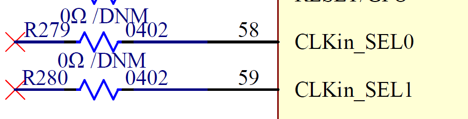
What is the recommended approach for implementing the clock selection logic when one clock is used as the primary source and the other as a backup—hardware-based or software-based?

Best Regards,

Gaurav
Screenshot 2026-06-26 164511.png

  • Either approach is suitable and it's a matter of preference or application requirements, which is why we implemented it both ways. I'll list some tradeoffs to help you make your choice.

    Pros Cons
    Hardware-based pin-selection
    • No SPI programming required after initialization, minimizing SPI traffic and any SPI crosstalk on clean outputs
    • Could be tied to external mux/switch/relay for better noise isolation between CLKIN0 and CLKIN1 (think about the slight PPM offset spur for two 100MHz clocks)
    • With only two clocks, can utilize one pin as reference switching, and other pin as LOS for primary pin, entirely without SPI
    • Debug signals must be routed out of other pins like STATUS_LDx or RESET
    • Holdover entry is pin-controlled, so system must react quickly to loss of signal or loss of lock to avoid large phase hits from sudden signal loss
    • No robustness advantages over SPI control (the register selecting pin-mode or software mode is just as susceptible to corruption as the register selecting which reference input to use)
    • More GPIO routing required from controller and very slight increase to BOM cost vs. not using CLKIN_SELx pins
    Software-based pin selection
    • CLKIN_SELx pins may be utilized as GPIO for debug/SPI/etc
    • Can take advantage of automatic reference selection, which may not require SPI at all in many cases
    • Less GPIO/routing required from control device if CLKIN_SELx pins are unused
    • Controller handles reference switching, requiring additional bus traffic, potential for crosstalk, more firmware work, etc
    • If automatic clock switching on loss of lock is not used, holdover entry is still manual, requiring a SPI write to enter holdover; this could be slower than GPIO due to 20MHz SPI clock and 24-bit register writes
    • Automatic clock switching on loss of SIGNAL (rather than loss of lock) requires configuring inputs in MOS mode, which can interfere with DC-coupled termination (e.g. can't put 100Ω directly across pins)