LMK1D1204: LMK1D1204 Single-ended Input Configuration

Part Number: LMK1D1204
Other Parts Discussed in Thread: LMK04832

Hi TI Team,
 
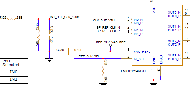
I am using the LMK1D1204 with a single-ended LVCMOS clock input. In my design, the LVCMOS signal is connected to IN− (N) and the bias voltage is applied to IN+ (P). The datasheet recommends connecting the signal to IN+ and the bias to IN−.
 
Could you please clarify:
1) Is this input configuration supported or expected to operate reliably?
2) Will the LVDS outputs simply be inverted (180° phase shift), or are there any other functional or performance implications?
3)The LVDS outputs are connected to the LMK04832 LVDS inputs. Is there any concern with this configuration?
 
Could you please Reply as soon as possible??
 
Thank you for your support.image.png
  • Hi Kethan,

    1) Is this input configuration supported or expected to operate reliably?

    Yes, this input configuration is supported.

    2) Will the LVDS outputs simply be inverted (180° phase shift), or are there any other functional or performance implications?

    Yes, the outputs will have a 180 degree phase shift applied.

    3)The LVDS outputs are connected to the LMK04832 LVDS inputs. Is there any concern with this configuration?

    No, that should be fine. 

    I am a bit puzzled by your input circuit, though. It seems you are AC coupling the VAC_REF output, which would then mean that the input signal is not being biased? The IN_N should be an LVCMOS/SE signal that swings from 0V to your VDD voltage, and the IN_P should be biased to the exact middle of that swing range (VDD/2).

    Thanks,

    Michael

  • Hi Michael,
    Thank you for your quick response and clarification.
    The capacitor is actually a decoupling capacitor for the VAC_REF0 output. The IN_P input is biased to VDD/2, and the LVCMOS clock is applied to IN_N.
    Thanks again for your support.
  • Ah, I see. That should be fine then.

    Thanks,

    Michael