LMX1860-SEP: SYSREF Outputs Latche Up to VCC at 660 kHz

Part Number: LMX1860-SEP

Hi,

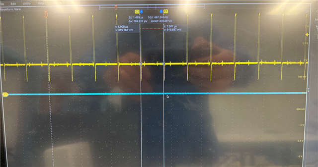
We observe bizarre behavior with LMX1860-SEP. As soon as the SYSREF_EN pin is asserted hi, the device outputs pulses to VCC on its SYSREF output channels. The pulses are not valid LVDS or CML pulses -- the two polarities (P & N) move together, rather than complimentarily (see scope shot). This is before any SPI Configuration whatsoever. Furthermore, the device will do this without a valid clock signal on clk_in P / N. To make matters worse, the device seems to not accept any SPI configuration with SYSREF_EN asserted hi. We have probed VCC --  it is stable at 2.5V. Our logic signals (SYSREF, MUXOUT_SEL, etc) are all 1.8V logic. 


Any guideance on this issue is greatly appreciated!
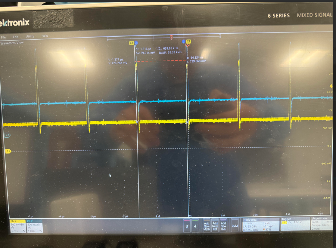
image.png


  • We're also noticing that if all of the outputs are disabled, then we can use configure the chip and use the logic sysref normally. However, having SYSREF_EN hi and any of the output channels active, we notice the problem occurring. The register SYSREF_EN can be cleared while the HW SYSREF_EN is set, which allows configuration of the chip. However if any of the channels are enabled when both the SYSREF_EN pin and register bit are set, the problem occurs. 

  • Adding to my last note, it actually seems like the issue occurs if any of the SYSREF outputs are enabled, besides LOGICSYSREF. Having the CLKOUTx_EN set is fine. Having any SYSREFOUTx_EN set with the global SYSREF_EN set causes the problem to occur. 

  • Another item I'll add, drving the SYSREFREQ pin has no effect on this issue. The issue appears regardless of the SYSREFREQ frequency or those pins are quiescent. The frequency of the common-mode toggles remains the same regardless of SYSREFREQ. 

  • I'm attaching a register set that works (lmx1860a.txt) and a register set that if you program the device with afterwards (lmx1860b.txt) causes the failure mode shown above. Regardless, coming from POR with SYSREF_EN enable and any of the outputs enable, the device demonstrates this failure mode as well. 

    R90	0x5A0000
    R86	0x560004
    R79	0x4F0205
    R76	0x4C0000
    R75	0x4B0003
    R72	0x480000
    R65	0x4165F0
    R29	0x1D05FF
    R28	0x1C0A08
    R25	0x190119
    R24	0x180001
    R23	0x17E040
    R22	0x16086F
    R21	0x152178
    R20	0x140EF8
    R19	0x130EF8
    R18	0x120EF8
    R17	0x110074
    R16	0x101140
    R15	0x0F0B80
    R14	0x0E0002
    R13	0x0D0003
    R12	0x0C0000
    R11	0x0B0000
    R9	0x09802E
    R8	0x080130
    R7	0x070001
    R6	0x06C924
    R5	0x05493F
    R4	0x043FFF
    R3	0x030F87
    R2	0x020223
    R0	0x000000
    
    R90	0x5A0000
    R86	0x560004
    R79	0x4F0205
    R76	0x4C0000
    R75	0x4B0003
    R72	0x480000
    R65	0x4165F0
    R29	0x1D05FF
    R28	0x1C0A08
    R25	0x190119
    R24	0x180001
    R23	0x17E040
    R22	0x16086F
    R21	0x152178
    R20	0x140EF8
    R19	0x130EF8
    R18	0x120EF8
    R17	0x110074
    R16	0x101140
    R15	0x0F0B80
    R14	0x0E0002
    R13	0x0D0003
    R12	0x0C0000
    R11	0x0B0000
    R9	0x09802E
    R8	0x080130
    R7	0x070001
    R6	0x06C924
    R5	0x05493F
    R4	0x043FFF
    R3	0x031F87
    R2	0x020223
    R0	0x000000
    

  • Hi There,

    After a Vcc power up, the device is in buffer mode, sysref is disabled, there should be no signal output from any sysref output port.

    Your configurations look fine. I have also tried both, I don't see any issue. Although sysref is enabled, if there is no SYSREFREQ signal, sysref output port remains silent. 

    The device can consume over 1A of current, make sure your power supply has sufficient current supply. 

    To put the device in full SPI control mode, verify the following pins have been strapped properly.

  • Hi,

    Our power supply has a current limit of 1.95A. We are using 1.8V CMOS logic from an FPGA to drive CLKx_EN, SYSREF_EN, CE, and LOGICEN. Per the datasheet, we thought that the min VIH of these pins was 1.4V, so we figured 1.8V was sufficient. Can you confirm that 1.8V on CLKx_EN, SYSREF_EN, CE, and LOGICEN is sufficient? 

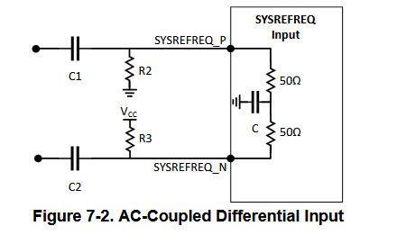
    Also we are biasing SYSREFREQ according to Figure 7.2 with R3 499 and R2 1K with nothing driving the network. Is this OK? 

    Could this problem be caused by unterminated CLKOUTx or SYSREFOUTx ports? Even if they're not powered on? 

    Thanks! 

  • Adding some more information: 

    I am able to reproduce the issue immediately by doing the following: 

    1. Power on the device with a 50 ohm load on both polarities of channel 0. The other channels are unterminated. 
    2. Set CE, SYSREF_EN, CLK0_EN, LOGIC_EN to 1.8V. 
    3. CLK1_EN, CLK2_EN, CLK3_EN are all driven to GND. 
    4. PWRSELx, DIVSELx, and MUXSELx are all pulled to GND permanently through 1k resistors. 
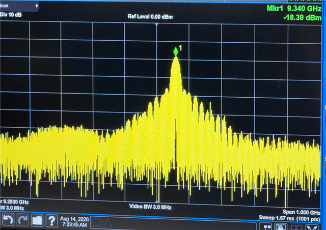
    5. Active the CLKIN signal source, LMX2694 outputting 9340 GHz with power set to 31. 
    6. Write the attached .txt file to the device. 
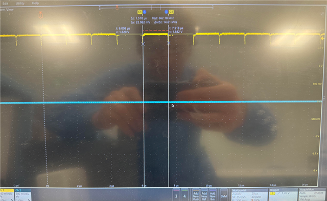
    7. Observe common mode pulses on LOGICSYSREF and SYSREFOUT0. Pulses also appear on disabled SYSREFOUT channels, but they look different. 

    Also note the RF output (RFOUT0) is apparently modulated by the ~660 kHz pulse train. 

    SYSREFOUT0 (enabled) 

    SYSREFOUT1 (disabled) 

    LOGICSYSREFOUT

    R90	0x5A0000
    R86	0x560004
    R79	0x4F0205
    R76	0x4C0000
    R75	0x4B0003
    R72	0x480000
    R65	0x4165F0
    R29	0x1D05FF
    R28	0x1C0A08
    R25	0x190119
    R24	0x180001
    R23	0x17E040
    R22	0x16086F
    R21	0x152178
    R20	0x140EF8
    R19	0x130EF8
    R18	0x120EF8
    R17	0x110074
    R16	0x101140
    R15	0x0F0B80
    R14	0x0E0002
    R13	0x0D0003
    R12	0x0C0000
    R11	0x0B0000
    R9	0x098008
    R8	0x080130
    R7	0x070001
    R6	0x06924B
    R5	0x0536FF
    R4	0x0438FF
    R3	0x031F87
    R2	0x020223
    R0	0x000000