LMK05318B: Unexpected 1PPS Phase Offset Between PRIREF and OUT7

Part Number: LMK05318B
Other Parts Discussed in Thread: LMK5B33216, LMK5C33216A

Hello,

Please provide guidance on the following functionality:
LMK05318B Data Sheet
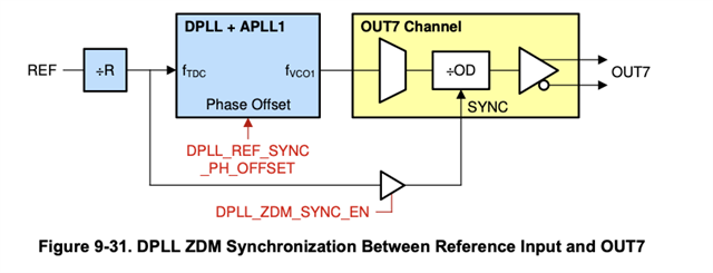
Section 8.3.16: 1PPS Input-to-Output Phase Alignment (PRIREF-to-OUT7 SYNC)

As an initial step, we configure the device as follows:
 - R252[7] DPLL_REF_SYNC_OUT7_EN = 0b1
 - R340 to R345 DPLL_REF_SYNC_PH_OFFSET = 0x0

We then perform a PLL reset using the following sequence:
 - R12[7] RESET_SW = 0b1
 - Wait 1 second
 - R12[7] RESET_SW = 0b0

We expect the OUT7 1PPS signal to be aligned with the PRIREF 1PPS signal within a few nanoseconds. However, the phase difference between PRIREF 1PPS and OUT7 1PPS is approximately -200 µs to -500 µs.
Immediately after the software reset is released, the first pulse has a phase difference of within +10 ns. However, it appears that the phase difference becomes significantly larger at some point afterward.
The phase difference changes to either approximately -200 µs or -500 µs each time a software reset is performed. Once it settles, however, it remains fixed at either -200 µs or -500 µs; it does not continuously vary between these values.
This behavior appears to indicate that the PLL locks after adjusting some kind of offset phase.
Could you please explain why the device behaves this way?
Also, please advise us which parameters need to be configured in order to achieve the expected phase alignment.

Best regards,
T.Serizawa

  • Hello, 

    Can you also try to set DPLL_REF_SYNC_OUT7_NDIV_RST_DIS = 1 and see if that improves the device behavior? Usually for 1pps phase alignment we recommend having this bit set along with DPLL_REF_SYNC_OUT7_EN. 

  • I accidentally asked my question under a related question.
    Please reply here.
    --------------
    I tried adding the setting DPLL_REF_SYNC_OUT7_NDIV_RST_DIS = 1 while leaving the other parameters unchanged, but this did not improve the operation. Are there any other parameters that need to be configured?


    As mentioned previously, the phase difference immediately after releasing SW_RESET is limited to approximately +10 ns. We expect this phase relationship to be maintained. Is it possible that an OFFSET value is being applied unintentionally?


    Additionally, we measured the unintended phase difference using multiple DUTs and observed different values for each DUT. From a circuit-design perspective, are there any factors that could affect the phase offset?


    As a supplementary note, I should have clarified that a GNSS-referenced 1PPS signal is being input to PRIREF. We are checking the phase against an external reference signal, and since the phase variation during the test is only a few nanoseconds, we believe that the stability of PRIREF is sufficient.

  • Hi Serizawa, 

    Since the initial phase error is only around 10ns and the steady state phase error is much wider, I wonder if it's possible that the DPLL is not locking properly. Can you try the debug steps below and see if any of these help?

    • Monitor the DPLL LOFL and LOPL status to confirm that the DPLL is reporting lock
    • Monitor the value of PLL1_NUM_STAT during DPLL lock acquisition. Ideally this value should be reasonably close to PLL1_NUM. This will essentially provide information on the measured frequency delta between the XO input and 1pps input 
    • Set R303[0] = 0. This can sometimes help improve the lock behavior for low frequency inputs (<2kHz)
    • Readback R345 to R340 to confirm that no phase offset value is being applied 

    My expectation is that with 1pps input-to-output alignment enabled and a phase offset of 0, the steady state error should only be a few ns and there should not be too much variance from device to device. 

  • Thank you for your response.

    - `LOFL` and `LOPL` indicate that the DPLL is locked.
    - We observed a difference between `PLL1_NUM_STAT` and `PLL1_NUM`.
    - `R303[0] = 0` has already been configured, but we have not observed any improvement in the issue.
    - `R340` through `R345` are set to 0.

    Although this is different from the behavior suggested in your comments, we reconfigured the `OUT7 DIV` using TICS Pro, after which the 1PPS phase difference settled at approximately −26 µs.

    However, the issue that different phase differences are observed for each DUT has not been resolved.

    We have attached the register readback results obtained while maintaining the phase difference of approximately −26 µs. Could you please review them?

    The registers were read twice: once immediately after recovery from `SW_RESET`, and again five minutes later.

    ----- Register status ------

    R Address Data (Immediately After RESET_SW) Data (5 Minutes Later) Difference
    0 0x0000 0x10 0x10 TRUE
    1 0x0001 0x0B 0x0B TRUE
    2 0x0002 0x35 0x35 TRUE
    3 0x0003 0x42 0x42 TRUE
    4 0x0004 0x15 0x15 TRUE
    5 0x0005 0x05 0x05 TRUE
    6 0x0006 0x12 0x12 TRUE
    7 0x0007 0x21 0x21 TRUE
    8 0x0008 0x04 0x04 TRUE
    9 0x0009 0x10 0x10 TRUE
    10 0x000A 0xC8 0xC8 TRUE
    11 0x000B 0x00 0x00 TRUE
    12 0x000C 0x1B 0x1B TRUE
    13 0x000D 0x08 0x08 TRUE
    14 0x000E 0x00 0x00 TRUE
    15 0x000F 0x00 0x00 TRUE
    16 0x0010 0x00 0x00 TRUE
    17 0x0011 0x1D 0x1D TRUE
    18 0x0012 0xFF 0xFF TRUE
    19 0x0013 0x0D 0x0D TRUE
    20 0x0014 0xF8 0xF8 TRUE
    21 0x0015 0x01 0x01 TRUE
    22 0x0016 0x00 0x00 TRUE
    23 0x0017 0x55 0x55 TRUE
    24 0x0018 0x55 0x55 TRUE
    25 0x0019 0x00 0x00 TRUE
    26 0x001A 0x00 0x00 TRUE
    27 0x001B 0x00 0x00 TRUE
    28 0x001C 0x01 0x01 TRUE
    29 0x001D 0x13 0x13 TRUE
    30 0x001E 0x40 0x40 TRUE
    31 0x001F 0x00 0x00 TRUE
    32 0x0020 0x44 0x44 TRUE
    33 0x0021 0x00 0x00 TRUE
    34 0x0022 0x00 0x00 TRUE
    35 0x0023 0x00 0x00 TRUE
    36 0x0024 0x03 0x03 TRUE
    37 0x0025 0x00 0x00 TRUE
    38 0x0026 0x00 0x00 TRUE
    39 0x0027 0x02 0x02 TRUE
    40 0x0028 0x0F 0x0F TRUE
    41 0x0029 0x00 0x00 TRUE
    42 0x002A 0x01 0x01 TRUE
    43 0x002B 0xC2 0xC2 TRUE
    44 0x002C 0x00 0x00 TRUE
    45 0x002D 0x00 0x00 TRUE
    46 0x002E 0x88 0x88 TRUE
    47 0x002F 0x07 0x07 TRUE
    48 0x0030 0x50 0x50 TRUE
    49 0x0031 0x4A 0x4A TRUE
    50 0x0032 0x00 0x00 TRUE
    51 0x0033 0x10 0x10 TRUE
    52 0x0034 0x10 0x10 TRUE
    53 0x0035 0x31 0x31 TRUE
    54 0x0036 0x10 0x10 TRUE
    55 0x0037 0x00 0x00 TRUE
    56 0x0038 0x31 0x31 TRUE
    57 0x0039 0x3C 0x3C TRUE
    58 0x003A 0x31 0x31 TRUE
    59 0x003B 0x3C 0x3C TRUE
    60 0x003C 0xF9 0xF9 TRUE
    61 0x003D 0x00 0x00 TRUE
    62 0x003E 0xF9 0xF9 TRUE
    63 0x003F 0x3C 0x3C TRUE
    64 0x0040 0x95 0x95 TRUE
    65 0x0041 0x02 0x02 TRUE
    66 0x0042 0xF8 0xF8 TRUE
    67 0x0043 0xFF 0xFF TRUE
    68 0x0044 0x0B 0x0B TRUE
    69 0x0045 0x00 0x00 TRUE
    70 0x0046 0x00 0x00 TRUE
    71 0x0047 0x20 0x20 TRUE
    72 0x0048 0x2F 0x2F TRUE
    73 0x0049 0x00 0x00 TRUE
    74 0x004A 0x00 0x00 TRUE
    75 0x004B 0x00 0x00 TRUE
    76 0x004C 0x00 0x00 TRUE
    77 0x004D 0x0F 0x0F TRUE
    78 0x004E 0x00 0x00 TRUE
    79 0x004F 0x11 0x11 TRUE
    80 0x0050 0x80 0x80 TRUE
    81 0x0051 0x0A 0x0A TRUE
    82 0x0052 0x00 0x00 TRUE
    83 0x0053 0x05 0x05 TRUE
    84 0x0054 0xA0 0xA0 TRUE
    85 0x0055 0x00 0x00 TRUE
    86 0x0056 0x00 0x00 TRUE
    87 0x0057 0x1E 0x1E TRUE
    88 0x0058 0x84 0x84 TRUE
    89 0x0059 0x80 0x80 TRUE
    90 0x005A 0x00 0x00 TRUE
    91 0x005B 0x14 0x14 TRUE
    92 0x005C 0x00 0x00 TRUE
    93 0x005D 0x05 0x05 TRUE
    94 0x005E 0xA0 0xA0 TRUE
    95 0x005F 0x00 0x00 TRUE
    96 0x0060 0x00 0x00 TRUE
    97 0x0061 0x1E 0x1E TRUE
    98 0x0062 0x84 0x84 TRUE
    99 0x0063 0x80 0x80 TRUE
    100 0x0064 0x29 0x29 TRUE
    101 0x0065 0x01 0x01 TRUE
    102 0x0066 0x22 0x22 TRUE
    103 0x0067 0x0F 0x0F TRUE
    104 0x0068 0x1F 0x1F TRUE
    105 0x0069 0x05 0x05 TRUE
    106 0x006A 0x00 0x00 TRUE
    107 0x006B 0x64 0x64 TRUE
    108 0x006C 0x00 0x00 TRUE
    109 0x006D 0x82 0x82 TRUE
    110 0x006E 0x35 0x35 TRUE
    111 0x006F 0x55 0x55 TRUE
    112 0x0070 0x55 0x55 TRUE
    113 0x0071 0x55 0x55 TRUE
    114 0x0072 0x55 0x55 TRUE
    115 0x0073 0x03 0x03 TRUE
    116 0x0074 0x01 0x01 TRUE
    117 0x0075 0x00 0x00 TRUE
    118 0x0076 0x00 0x00 TRUE
    119 0x0077 0x00 0x00 TRUE
    120 0x0078 0x00 0x00 TRUE
    121 0x0079 0x00 0x00 TRUE
    122 0x007A 0x00 0x00 TRUE
    123 0x007B 0x35 0x35 TRUE
    124 0x007C 0x56 0x56 TRUE
    125 0x007D 0x01 0x00 FALSE
    126 0x007E 0x96 0xCF FALSE
    127 0x007F 0x08 0x46 FALSE
    128 0x0080 0x00 0x00 TRUE
    129 0x0081 0x08 0x08 TRUE
    130 0x0082 0x00 0x00 TRUE
    131 0x0083 0x3C 0x3C TRUE
    132 0x0084 0x3C 0x3C TRUE
    133 0x0085 0x77 0x77 TRUE
    134 0x0086 0x00 0x00 TRUE
    135 0x0087 0x2B 0x2B TRUE
    136 0x0088 0x00 0x00 TRUE
    137 0x0089 0x28 0x28 TRUE
    138 0x008A 0xE5 0xE5 TRUE
    139 0x008B 0x03 0x03 TRUE
    140 0x008C 0x02 0x02 TRUE
    141 0x008D 0x00 0x00 TRUE
    142 0x008E 0x01 0x01 TRUE
    143 0x008F 0x01 0x01 TRUE
    144 0x0090 0x77 0x77 TRUE
    145 0x0091 0x01 0x01 TRUE
    146 0x0092 0x89 0x89 TRUE
    147 0x0093 0x20 0x20 TRUE
    148 0x0094 0x86 0x86 TRUE
    149 0x0095 0x0D 0x0D TRUE
    150 0x0096 0x00 0x00 TRUE
    151 0x0097 0x01 0x01 TRUE
    152 0x0098 0x0D 0x0D TRUE
    153 0x0099 0x29 0x29 TRUE
    154 0x009A 0x24 0x24 TRUE
    155 0x009B 0x7C 0x7C TRUE
    156 0x009C 0x01 0x01 TRUE
    157 0x009D 0x00 0x00 TRUE
    158 0x009E 0x00 0x00 TRUE
    159 0x009F 0x00 0x00 TRUE
    160 0x00A0 0xFC 0xFC TRUE
    161 0x00A1 0x00 0x7C FALSE
    162 0x00A2 0x00 0xC7 FALSE
    163 0x00A3 0xC5 0xF0 FALSE
    164 0x00A4 0x00 0x00 TRUE
    165 0x00A5 0x00 0x00 TRUE
    166 0x00A6 0x00 0x00 TRUE
    167 0x00A7 0x01 0x01 TRUE
    168 0x00A8 0x06 0x06 TRUE
    169 0x00A9 0x00 0x00 TRUE
    170 0x00AA 0x00 0x00 TRUE
    171 0x00AB 0x00 0x00 TRUE
    172 0x00AC 0x00 0x00 TRUE
    173 0x00AD 0x00 0x00 TRUE
    174 0x00AE 0x00 0x00 TRUE
    175 0x00AF 0x00 0x00 TRUE
    176 0x00B0 0x00 0x00 TRUE
    177 0x00B1 0x00 0x00 TRUE
    178 0x00B2 0x00 0x00 TRUE
    179 0x00B3 0x00 0x00 TRUE
    180 0x00B4 0x00 0x00 TRUE
    181 0x00B5 0x00 0x00 TRUE
    182 0x00B6 0x00 0x00 TRUE
    183 0x00B7 0x00 0x00 TRUE
    184 0x00B8 0x00 0x00 TRUE
    185 0x00B9 0xF5 0xF5 TRUE
    186 0x00BA 0x01 0x01 TRUE
    187 0x00BB 0x00 0x00 TRUE
    188 0x00BC 0x00 0x00 TRUE
    189 0x00BD 0x00 0x00 TRUE
    190 0x00BE 0x00 0x00 TRUE
    191 0x00BF 0x00 0x00 TRUE
    192 0x00C0 0x50 0x50 TRUE
    193 0x00C1 0x18 0x18 TRUE
    194 0x00C2 0x00 0x00 TRUE
    195 0x00C3 0x00 0x00 TRUE
    196 0x00C4 0x00 0x00 TRUE
    197 0x00C5 0x1D 0x1D TRUE
    198 0x00C6 0x00 0x00 TRUE
    199 0x00C7 0x00 0x00 TRUE
    200 0x00C8 0x1D 0x1D TRUE
    201 0x00C9 0x00 0x00 TRUE
    202 0x00CA 0x00 0x00 TRUE
    203 0x00CB 0x00 0x00 TRUE
    204 0x00CC 0x15 0x15 TRUE
    205 0x00CD 0x00 0x00 TRUE
    206 0x00CE 0x00 0x00 TRUE
    207 0x00CF 0x15 0x15 TRUE
    208 0x00D0 0x00 0x00 TRUE
    209 0x00D1 0x14 0x14 TRUE
    210 0x00D2 0x00 0x00 TRUE
    211 0x00D3 0x16 0x16 TRUE
    212 0x00D4 0x00 0x00 TRUE
    213 0x00D5 0x14 0x14 TRUE
    214 0x00D6 0x00 0x00 TRUE
    215 0x00D7 0x16 0x16 TRUE
    216 0x00D8 0x00 0x00 TRUE
    217 0x00D9 0x00 0x00 TRUE
    218 0x00DA 0x03 0x03 TRUE
    219 0x00DB 0xF9 0xF9 TRUE
    220 0x00DC 0x41 0x41 TRUE
    221 0x00DD 0x00 0x00 TRUE
    222 0x00DE 0x02 0x02 TRUE
    223 0x00DF 0x08 0x08 TRUE
    224 0x00E0 0xD6 0xD6 TRUE
    225 0x00E1 0x00 0x00 TRUE
    226 0x00E2 0x03 0x03 TRUE
    227 0x00E3 0xF9 0xF9 TRUE
    228 0x00E4 0x41 0x41 TRUE
    229 0x00E5 0x00 0x00 TRUE
    230 0x00E6 0x02 0x02 TRUE
    231 0x00E7 0x08 0x08 TRUE
    232 0x00E8 0xD6 0xD6 TRUE
    233 0x00E9 0x10 0x10 TRUE
    234 0x00EA 0x10 0x10 TRUE
    235 0x00EB 0x01 0x01 TRUE
    236 0x00EC 0x24 0x24 TRUE
    237 0x00ED 0xF8 0xF8 TRUE
    238 0x00EE 0x00 0x00 TRUE
    239 0x00EF 0x00 0x00 TRUE
    240 0x00F0 0xC3 0xC3 TRUE
    241 0x00F1 0x50 0x50 TRUE
    242 0x00F2 0x00 0x00 TRUE
    243 0x00F3 0x3F 0x3F TRUE
    244 0x00F4 0x00 0x00 TRUE
    245 0x00F5 0x00 0x00 TRUE
    246 0x00F6 0x00 0x00 TRUE
    247 0x00F7 0x00 0x00 TRUE
    248 0x00F8 0x00 0x00 TRUE
    249 0x00F9 0x21 0x21 TRUE
    250 0x00FA 0x00 0x00 TRUE
    251 0x00FB 0x03 0x03 TRUE
    252 0x00FC 0xE9 0xE9 TRUE
    253 0x00FD 0x12 0x12 TRUE
    254 0x00FE 0x06 0x06 TRUE
    255 0x00FF 0xFC 0xFC TRUE
    256 0x0100 0x00 0x00 TRUE
    257 0x0101 0x01 0x01 TRUE
    258 0x0102 0x00 0x00 TRUE
    259 0x0103 0x01 0x01 TRUE
    260 0x0104 0x02 0x02 TRUE
    261 0x0105 0x80 0x80 TRUE
    262 0x0106 0x01 0x01 TRUE
    263 0x0107 0x2A 0x2A TRUE
    264 0x0108 0x05 0x05 TRUE
    265 0x0109 0xF2 0xF2 TRUE
    266 0x010A 0x00 0x00 TRUE
    267 0x010B 0xA0 0xA0 TRUE
    268 0x010C 0x04 0x04 TRUE
    269 0x010D 0x00 0x00 TRUE
    270 0x010E 0x02 0x02 TRUE
    271 0x010F 0x56 0x56 TRUE
    272 0x0110 0x1F 0x1F TRUE
    273 0x0111 0x1B 0x1B TRUE
    274 0x0112 0x1B 0x1B TRUE
    275 0x0113 0x1D 0x1D TRUE
    276 0x0114 0x1F 0x1F TRUE
    277 0x0115 0x1F 0x1F TRUE
    278 0x0116 0x00 0x00 TRUE
    279 0x0117 0x00 0x00 TRUE
    280 0x0118 0x00 0x00 TRUE
    281 0x0119 0x00 0x00 TRUE
    282 0x011A 0x00 0x00 TRUE
    283 0x011B 0x00 0x00 TRUE
    284 0x011C 0x08 0x08 TRUE
    285 0x011D 0x08 0x08 TRUE
    286 0x011E 0x00 0x00 TRUE
    287 0x011F 0x00 0x00 TRUE
    288 0x0120 0x00 0x00 TRUE
    289 0x0121 0x00 0x00 TRUE
    290 0x0122 0x02 0x02 TRUE
    291 0x0123 0x01 0x01 TRUE
    292 0x0124 0x00 0x00 TRUE
    293 0x0125 0x01 0x01 TRUE
    294 0x0126 0x00 0x00 TRUE
    295 0x0127 0x21 0x21 TRUE
    296 0x0128 0x02 0x02 TRUE
    297 0x0129 0x00 0x00 TRUE
    298 0x012A 0x00 0x00 TRUE
    299 0x012B 0x01 0x01 TRUE
    300 0x012C 0x00 0x00 TRUE
    301 0x012D 0x14 0x14 TRUE
    302 0x012E 0x17 0x17 TRUE
    303 0x012F 0x00 0x00 TRUE
    304 0x0130 0x0F 0x0F TRUE
    305 0x0131 0x04 0x04 TRUE
    306 0x0132 0x61 0x61 TRUE
    307 0x0133 0xF8 0xF8 TRUE
    308 0x0134 0x43 0x43 TRUE
    309 0x0135 0xC3 0xC3 TRUE
    310 0x0136 0xC3 0xC3 TRUE
    311 0x0137 0xC3 0xC3 TRUE
    312 0x0138 0xC3 0xC3 TRUE
    313 0x0139 0xC3 0xC3 TRUE
    314 0x013A 0xFF 0xFF TRUE
    315 0x013B 0xFF 0xFF TRUE
    316 0x013C 0xFF 0xFF TRUE
    317 0x013D 0xFF 0xFF TRUE
    318 0x013E 0xFF 0xFF TRUE
    319 0x013F 0x02 0x02 TRUE
    320 0x0140 0x00 0x00 TRUE
    321 0x0141 0x0A 0x0A TRUE
    322 0x0142 0x00 0x00 TRUE
    323 0x0143 0x00 0x00 TRUE
    324 0x0144 0x00 0x00 TRUE
    325 0x0145 0x01 0x01 TRUE
    326 0x0146 0x06 0x06 TRUE
    327 0x0147 0x35 0x35 TRUE
    328 0x0148 0x75 0x75 TRUE
    329 0x0149 0x0B 0x0B TRUE
    330 0x014A 0x00 0x00 TRUE
    331 0x014B 0x64 0x64 TRUE
    332 0x014C 0x00 0x00 TRUE
    333 0x014D 0x00 0x00 TRUE
    334 0x014E 0x3D 0x3D TRUE
    335 0x014F 0x09 0x09 TRUE
    336 0x0150 0x06 0x06 TRUE
    337 0x0151 0x35 0x35 TRUE
    338 0x0152 0x75 0x75 TRUE
    339 0x0153 0x0B 0x0B TRUE
    340 0x0154 0x00 0x00 TRUE
    341 0x0155 0x00 0x00 TRUE
    342 0x0156 0x00 0x00 TRUE
    343 0x0157 0x00 0x00 TRUE
    344 0x0158 0x00 0x00 TRUE
    345 0x0159 0x00 0x00 TRUE
    346 0x015A 0x02 0x02 TRUE
    347 0x015B 0x00 0x00 TRUE
    348 0x015C 0x00 0x00 TRUE
    349 0x015D 0x00 0x00 TRUE
    350 0x015E 0x00 0x00 TRUE
    351 0x015F 0x00 0x00 TRUE
    352 0x0160 0x00 0x00 TRUE
    357 0x0165 0x28 0x28 TRUE
    367 0x016F 0x00 0x00 TRUE
    411 0x019B 0x04 0x04 TRUE

  • Hi Serizawa, 

    Thanks for sending over the register readback, it looks like everything should be configured for the 1pps input-to-output alignment feature to work correctly. I'll take a look into this on my bench setup to see if I can replicate the same behavior that you're observing, I should be able to get back to you with more feedback in the next 1-2 days. 

  • Hi Serizawa, 

    I tested your register configuration on my setup, and I saw that the input-to-output 1pps phase offset converged close to 50ns after the DPLL had been locked for several minutes. Note that I loaded your exact register map except for register R148, as this is a reserved register which stores some calibrated trim values that are unique for each specific DUT. Based on this I don't believe there are any issues with the device configuration, but there could be some issue with the 1pps measurement setup. 

  • Hi Serizawa and Conner,

    R303 was mentioned and depending on Tics Pro version there was an optimization that was later undone.
    TICS Pro "Run Script" overrides 1PPS optimization


    4 months ago "R303 should be set to 0 to lock to 1pps, and it should be set to 1 for high frequency inputs. Currently the DPLL script will always overwrite R303 as 1 regardless of the actual input frequency. We are planning to update TICS Pro to handle this automatically, but first we will do some further testing to find the optimal threshold of the input frequency to switch this between 0 vs. 1.

    In general, for 1pps inputs I expect optimal lock behavior after running the script in TICS Pro to set the desired XO frequency and DPLL LBW, and manually setting R303 = 0."


  • Hi Octo, 

    Thanks for the comment, we are still recommending setting R303 = 0 for 1pps inputs. 

  • Thank you for your response.


    We would like to reconfirm the procedure for applying the settings.


    We are applying the configuration values from the .tcs file generated by TICS Pro as-is. After configuring the device, we write 0x9B to R12 (Offset = 0xC), wait for one second, and then perform a software reset by writing 0x1B.


    Is this procedure complete and correct, or are there any missing or unnecessary steps?


    We have applied the same procedure and the same .tcs file settings to several test devices. However, we have observed different phase differences between PRIREF and OUT7: 50 ns on some devices, 26 µs on others, and 50 ms on others.


    If you are aware of any deficiencies or issues in the hardware design that could lead to this type of behavior, we would appreciate it if you could point them out.

  • Hi Serizawa,

    The sequence for softreset you mentioned is correct and complete.

    About the phase differences observed between devices or between power cycles.
    Try R252[7:6] = 0x03

    The LMK05318B has support for pseudo Zero Delay Mode ZDM by resetting the output divider, it is not a feedback from the OUT7.
    Output phase will be deterministic within one VCO cycle and OUT7 must be derived from DPLL + APLL1.
    If this phase deviation is still too high I would suggest the LMK5B33216 device series.


    For best phase lock behavior on 1 PPS, manually set R303[7:0] = 0x00 as you will find 0x01 in the TICS Pro output (HexRegisterValues file).

  • Hi Serizawa, 

    In addition to Octo's comments, I would like to double check on other part of your programming procedure. Are you writing a fixed value to R148 in your programming sequence? If so, could you skip writing to this register? Like I mentioned in my previous reply, this register contains a calibration value to tune the BAW VCO center frequency and it is unique for each device. I suspect this could be the root cause of the issue that you're observing since there is so much variation from device to device. 

  • Thank you for your response.

    We double-checked whether any settings were applied to R148, and confirmed that we had not modified this register. This is presumably because we have been configuring the device based on the `.tcs` file provided by TICS Pro.

    However, we are not certain whether R148 has never been configured at any point. We understand that the device contains internal EEPROM. Is the value in this register cleared by a power-on reset? If it is not cleared, could you please advise us on how to restore the device-specific value?

    Thank you also for suggesting changes to the LMK5B33216. We are currently considering switching to the LMK5C33216A, taking into account the lower jitter and lower phase noise of the output clock. Can this device achieve similar results regarding phase alignment convergence, as with the LMK5B33216?

    For reference, the output clocks are 50 MHz, 10 MHz, and 1 PPS. Is it possible to generate these clocks using APLL3 (BAW VCO) on the LMK5C33216A?

  • Both devices share the same architecture and physical pinout and the difference lies in the frequency of the BAW oscillator.

    LMK5C33216A optimized for 491.52 MHz multiples.
    LMK5B33216 Optimized for 312.5 MHz / 625 MHz multiples.

    Snippet from Figure 8-1. (both datasheets) Top-Level Block Diagram

    For 50 MHz, 10 MHz, and 1 PPS output I think the LMK5B33216 will be the best match. Please correct me if I'm wrong Connor/Jennifer?
    Your required frequencies can all be derived from DPLL3/APLL3 and phase aligned to the 1PPS reference.

    For best performance we also have to consider the XO frequency to be non-integer related to the output frequencies to minimize spurious noise.
    XO = 24.576MHz for example.

  • Hi Serizawa, 

    That's correct, R148 is stored in the internal EEPROM and is cleared by a power-on-reset. 

    LMK5C33216A and LMK5B33216 are essentially the same device, the only difference is the BAW VCO frequency (2457.6MHz for LMK5CA, 2500MHz for LMK5B). Since the 50MHz and 10MHz output clocks can be easily divided from the 2500MHz VCO, I would recommend using LMK5B33216. 

  • Thank you for your response. I would like to confirm my understanding of the VCO calibration.
    Is the following understanding correct?
    R148 contains the setting/calibration value for the BAW VCO center frequency, and the factory-adjusted value is loaded from the EEPROM upon a Power-On Reset.
    It is possible for the operator to overwrite R148; however, this does not change the value stored in the EEPROM, so the overwritten value is cleared by the next Power-On Reset.
    In addition, could you please let us know whether there is any way to verify that the value in R148 is appropriate? For example, could we confirm the center frequency by outputting a signal above xxx GHz on OUTxx while the device is operating in free-running mode?

    I also appreciate your suggestions regarding the selection of the LMK5B33216.

  • Hi Serizawa, 

    Your understanding is correct. There's not a straightforward way to check if the value in R148 is appropriate, but one approach is to rail the VCO in a positive and negative direction and see how much margin there is around the nominal 2500MHz center frequency. For example, you could input an XO signal with a large negative or positive ppm offset and observe the output ppm. When the VCO rails in either direction, there should be at least +/-100 ppm tuning range in either direction from the 2500MHz nominal frequency. 

    Another approach is to lock the VCO to 2500MHz and measure the tuning voltage at the LF1 pin. At room temperature this is expected to be in the range of 1.1-1.3V. Let me know if you have any other questions on this. 

  • Thank you for your response. I have taken over this matter from Serizawa.

    When I checked register R148 read from the EEPROM, I found that it was set to 0x86. I tried changing this setting to values in the range of approximately 0x70 to 0xA0, where BAW LOCK converges, but this had no effect on the issue in which a 26-microsecond offset is inserted. I also measured the voltage on the LF1 pin and found it to be approximately 1.13 V, which appears to be within the expected range.

    Attached are the measured waveforms on the PRIREF and OUT7 pins when RESET_SW was executed by changing register 0x0C from 0x9B to 0x1B.

    In the video, register 0x50, bit 7 (BAW LOCK), remains 0b1 throughout. Register 0xA8, bit 1 (DPLL LOCK), transitions to 0b1 at approximately 0:40. Register 0xA8, bit 2 (DPLL PHASE LOCK), remains 0b0 throughout the video; however, it changes to 0b1 after the video ends. In addition, the phase relationship between PRIREF and OUT7 does not change.

  • Dear hidetaka,

    Maybe your XO frequency is drifting during first minutes.
    Do you use an OCXO?


    I was able to reproduce similar behavior.
    Custom board, LMK05318B,  XO=24.576MHz OCXO, 1PPS reference.
    First PPS pulse at out7 within about 10's of ns.
    Second and following PPS pulses with 67.2 ms offset. Solid at 67.2ms. DPLL freq+phase locked.

    How to reproduce at least 5 times:
    Custom board (hot OCXO) power interrupted for 30 seconds to let the OCXO cool down several degrees.
    PPS from GNSS continues with standby-power.

    My thoughts:
    After PRIREF validation the out7 unmuted and out7 divider is reset by the PRIREF pulse to get deterministic phase.
    The OCXO output frequency is not stable within the short ref validation period of 6.4 seconds. Still heating up.
    I believe that the (quasi) ZDM captures the PPS while rising/falling XO frequency.
    The LMK05318B has a ZDM implementation that works under certain conditions.

    With hot OCXO the phase was repeatable in the <50ns range.
    A controller soft-resets the LMK05318B after reaching stable working temperature or 5 minutes timeout period.

    Regards,
    Octo

  • Thank you for confirming the reproducibility.

    We are using the SiTime SIT5501AI-WUG33IT-19.200000F as the XO.

    We understand that similar behavior may occur when synchronization with the PPS is performed while the XO frequency is not stable. However, the issue can still be reproduced even when performing a software reset 30 minutes after powering on the device, when the XO frequency should have been sufficiently stable.

    We perform the software reset using the following control sequence. Does this procedure reset the functional blocks within the PLL that could be related to this issue?

    • 0xC = 0x1B → 0x9B → 0x1B

    As an additional experiment, we also tried the following procedure, but it did not improve the situation:

    1. Stop the GNSS_1PPS output.
    2. Apply the setting values previously provided by Serizawa.
    3. Wait 30 minutes after powering on the device.
    4. Start the GNSS_1PPS output.
  • Hi hidetaka,

    Interesting result.
    The oscillator startup time of SIT5501AI is typically 2.5 ms and Time to Rated Frequency Stability is <1.6 seconds.
    So there is no warmup problem expected that causes the phase offset.
    Somehow the ZDM condition is not met. I will do lab experiment today.

  • We would greatly appreciate it if you could conduct the experiment and share the results with us.

    As additional information, we checked whether any noticeable frequency drift occurred on the 19.2 MHz clock during the software reset, but no noticeable frequency drift was observed.

    We have attached the captured XO waveform (GREEN) during the software reset. BLUE and RED similarly represent PRIREF and OUT7, respectively.

  • Hi hidetaka,
    I did repeated power cycles with my custom board and every time the phase was predictable and stable.
    Conducted not all tests because the ethernet link was also clocked by the LMK and a soft-reset would lock me out.
    I'll get back to you tomorrow.

  • unfortunately took longer than expected because it cannot be investigated remotely, I'll follow-up tomorrow.

  • Hi hidetaka,

    Various tests were conducted, and the phase was predictable after each soft reset.
    42ns between PRIREF and OUT7.

    • soft reset R12  = 0x1B → 0x9B → 0x1B