LMK5B33216: Output Issue

Part Number: LMK5B33216

Hi Team,

I'm using the clock generator IC LMK5B33216RGCR in my board. The current board schematics is shared below.
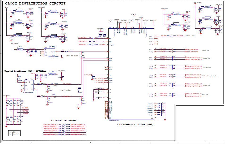
image.png

In the current schematic, the GPIO0 and GPIO2 signals are left unconnected. Initially, the I²C interface was not detecting the clock IC for programming.We then populated R143 and R139 to pull GPIO0 and GPIO2 to GND. After this change, the I²C interface was detected successfully, and we were able to program the clock IC.

Additionally, since we are using only the OCXO as the input clock source, the power supply components for IN0 and IN1 were initially kept DNP. However, with these components unpopulated, we were still unable to program the IC correctly.We then populated FB27, FB28, C346, C348, C342, C340, C343, and C172 to provide the required power to the VDD_IN0 and VDD_IN1 pins of the IC. After populating these components, the clock IC was successfully detected and programmed through the I²C interface.

Could you please check and clarify why populating these components is required for successful I²C detection and programming.

Regards,

Abhishek

  • Hi Abhishek, 

    VDD_IN0 and VDD_IN1 are required for this part for proper power conditioning, regardless if IN0 and IN1 are being used. Leaving a VDD-type pin floating can potentially cause unpredictable behavior, which can disrupt the digital core and I2C interface even though IN0/IN1 aren't functionally needed in APLL-only mode. The datasheet (see below) also implies that the ferrite bead component for these power supply pins can be omitted, but the underlying VDD_IN0/VDD_IN1 pin should still be tied to the supply rail rather than left floating. 

    Best,
    Jaryd

  • Hi Jaryd,

    Thanks for the confirmation. Please provide the feedback for the GPIO0 and GPIO2 connection also.

    In the current schematic, the GPIO0 and GPIO2 signals are left unconnected. Initially, the I²C interface was not detecting the clock IC for programming.We then populated R143 and R139 to pull GPIO0 and GPIO2 to GND. After this change, the I²C interface was detected successfully, and we were able to program the clock IC.

    Regards,

    Abhishek

  • Hi Abhishek, 

    The GPIO0 and GPIO2 pins are normally configured as 3-level inputs used to select the ROM page on start-up, so when these pins are left floating they may not settle reliably to a defined logic level (L/M/H) during POR. What may be happening is the device is latching to an indeterminate or unintended ROM page, including one that could potentially misconfigure the device such that the I2C interface doesn't come up correctly. Below are the voltage ranges for the L/M/H levels of the device. 

    Best,
    Jaryd