CDCE6214-Q1: CDCE6214

Part Number: CDCE6214-Q1
Other Parts Discussed in Thread: CDCE6214,

Hello, I would like to consult about the use of CDCE6214. At present, I cannot realize the control of CDCE6214 chip. In detail: In order to bypass the reading and writing of eeprom, only the register set of the chip is written. At the same time, HW_SW_CTRL and REFSEL have been connected to the MCU on the hardware circuit, so the IO pins connected to the MCU are configured to high resistance state to realize the dangling state of HW_SW_CTRL and REFSEL. Let the chip enter the backoff mode. The voltage of the two pins measured by the multimeter is 1.6V, so it is confirmed that the state is M and the backoff mode has been entered. Then I used IIC to write the CDCE6214RGER register, but after a lot of tests, only a few registers were written correctly, and the values of the other registers were not the values I set. For example, the operation of first pulling PDN and then reading and writing register R43 can realize the reading and writing of the register, which shows the timing correctness of IIC, but when writing other registers, most of them have errors. In addition, the register group values (R0-R85) are obtained by TICSPRO software. Therefore, I would like to ask if there is anything else I have not considered. I hope to get a reply,thank you.

  • Hello,

    Can you help restate the issue? 

    In fall back mode the I2C address should be 0x67. once you have made the updates through the TICS Pro tool i suggest that you issue a VCO recalibration and check lock status to ensure that the VCO is locked. 

    Before writing to the EEPROM i suggest looking at the output to ensure expected output is observed. 

    Following that you can use section 7.5 of the datasheet to program the device coupled with the EVM user Guide section 2.5 

    Best,

    Sandra

  • Thank you for your reply. Below is my more detailed design information. At present, I have only used HW_SW_CTRL, REFSEL, PDN, SCL/GPIO3, and I2C_SDA/GPIO2. HW_SW_CTRL and REFSEL are already in the M state, and the multimeter measured 1.6 V, which has been verified. For the PDN pin, I use an MCU GPIO to pull it low for reset and pull it high to start. SCL/GPIO3 and I2C_SDA/GPIO2 are used as the I2C clock and data lines. All other pins are unused. Could it be that other unused pins need to be used or configured in conjunction in order to achieve correct operation?

    On the software side, I implement read and write operations by programming the I2C timing on the MCU. For a write: the target address is 0x67; I shift the target address left by one bit and add the Wr bit, wait for ACK, then sequentially write Register Address High, wait for ACK, write Register Address Low, wait for ACK, write Data Byte High, wait for ACK, write Data Byte Low, wait for ACK, and then issue a STOP. The read timing also follows the datasheet.

    Currently, I have verified that register R43 can be read from and written to arbitrarily, which most likely indicates that the read/write timing is correct. However, when writing to other registers, many incorrect situations occur. By the way, a quick question: do all registers support read/write operations? The above is my more detailed question. My ultimate goal is to directly read from and write to registers R0–R85 without writing to the EEPROM, in order to achieve output at a specific frequency. I wonder whether I have missed any issues.

    Looking forward to your reply. Thank you....

  • Hi Linli,

    Not all of the CDCE6214 registers support read/write operations, as some are read-only registers. The register map for the CDCE6214-Q1 can be found here --> CDCE6214-Q1 Register Map User's Guide. Your I2C read/write sequence looks correct; could you confirm if the discrepancies you are seeing are from writing to read-only registers? 

    Additionally if you are writing all registers from a file, make sure to write in order from R85 to R0. R0 contains the I2C_A0 bit for the device I2C address and the recalibration and sync bits. As Sandra mentioned as well, we recommend to recalibrate the PLL after modification of the PLL settings (R0[4] = 1).

    Best,
    Jaryd

  • Hi Dukes,
    I have already downloaded and reviewed the CDCE6214-Q1 Register Map User's Guide. It does provide detailed descriptions of the register bits for R0–R85, including the read/write types supported by the registers. You are correct. I re-performed IIC read/write operations on the registers that fully support read/write, and they worked completely. For read-only registers, writing and then reading back produces anomalies. I understand that read-only registers cannot be written. However, I have a question: in the TICS Pro software, after adjusting all parameters according to my inputs and expected outputs, I can obtain the Raw register values for R0–R85 in the interface, but there are cases in which values are written to read-only registers or specific read-only bits. How should this be handled? For the generated values corresponding to certain read-only registers, or the value corresponding to a specific read-only bit, do I need to write them via IIC? If I directly use IIC to iterate through and write the R85–R0 register values generated by the TICS Pro software, but, due to the register read/write types, I cannot keep all register values consistent with those generated by the TICS Pro software, will this affect the operation of the CDCE6214?
    Best,
    Linli

  • Hi Linli,

    Glad to hear the read/write is working properly!

    You can write the entire image (R85 - R0) including the reserved and read-only addresses, but you should only verify the writable fields on readback. Any mismatches on the read-only and self clearing bits are expected and are not an error condition. 

    Best,
    Jaryd

  • Hi Dukes,

    I understand what you mean. I will try again to check if it is functioning properly. Thank you very much.

    Best,

    Linli

  • Hi Dukes,

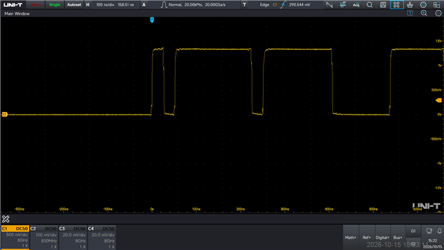
    After I attempted to write it, the resulting signal was a bit abnormal. After passing through the intermediate state, the signal eventually disappeared, which did not match the expected 10 MHz signal. The input was a 25 MHz square wave generated by the AWG, and it was observed using a scope as shown in the figure. The program involves writing to R85 to R0, and then calibrating by writing to R0[4]. Have I overlooked any steps?

    Best,

    Linli

  • Hi Linli,

    Could you describe a bit more what exactly you are measuring, and what signal is looking abnormal? Is this your reference into the CDCE6214, or is this the output? If the input is too noisy the device might not be locking to the reference; you can read back register R7[0] to determine if the PLL is locked to the reference or not. 

    Best,
    Jaryd