This thread has been locked.

If you have a related question, please click the "Ask a related question" button in the top right corner. The newly created question will be automatically linked to this question.

CDCV304 clock buffer unused pin

Other Parts Discussed in Thread: CDCV304, LMX2581

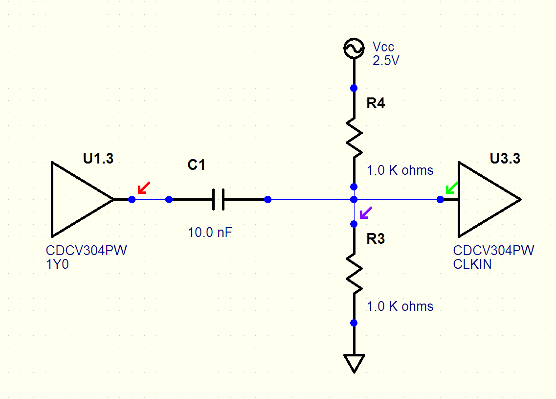
The CDCV304 clock output pins (Y0, Y1, Y2, Y3) if a pair is unused can i leave this pins unconnected or should I terminate it? If so what is the recommended termination scheme?  

Is there any performance degradation if I leave the unused pin no connect?

  • Hi Tony,

    the best way to treat the unsed LVCMOS outputs, is to leave them open/unconnected. If you terminate them, you will get a current flowing on the board which may cause crosstalk. Therefore, no performance degradation are expected.

    Best regards,

    Leandro 

  • Hi Leandro,

    If the CDCV304 is powered by 2.5v ,the output of the CDCV304 is should be LVCMOS2.5V, it is right ? If it is right ,the output  can be  directly connected the Virtex6 FPGA'bank (the bank's power supply is 2.5v).

    Best regards,

    Lei

  • Hi Lei,

    that is correct: if the CDCV304 is powered by 2.5V, its outputs will be 2.5V LVCMOS. Also your second statement is correct, you can DC couple the V304 output to the FPGA bank. DC coupling is usually OK for small board routing and if the two devices (CDCV304 and the FPGA in this case) share the same GND connection. AC coupling is usually require in case of long routing and if the two devices have different GND or GND levels.

    Best regards,

    Leandro

  • Hi Leandro,

    Thanks for you reply!

    1.For the DC coupling , it is needed to add a resistor between the output of the CDCV304 and the input of the FPGA,it is right ?

    2.For the AC coupling , it is needed to add a capacitance between the output of the CDCV304 and the input of the FPGA,it is right ?

    Best regards,

    Lei

  • Hi Lei,

    1. for DC coupling a 30Ohm series resistor is suggested for impedance matching with the 50Ohm transmission line

    2. for AC coupling a series cap is needed and after the cap you need to provide an appropriate bias voltage, which should be Vcc/2 for LVCMOS. The value of the capacitor can be in the 10nF range.

    Regards,

    Leandro

  • Hi Leandro,

    'For AC coupling a series cap is needed and after the cap you need to provide an appropriate bias voltage, which should be Vcc/2 for LVCMOS.' To the provide an appropriate bias voltage,that is why? the picture is followed ,is it right ?


    Regards,

    Lei


  • hi Lei,

    that's wrong. Please find attached a suggested connection. The U3.3 device is placed to emulate the FPGA clock input stage.

    Regards,

    Leandro

  • Hi Leandro,

    what is  the U3.3 device ? Accord to the picture , the divice U3.3 is CDCV304 . If  the divice U3.3 is CDCV304 ,i am confused. The CDCV304's output as a input of the cdcv304.  If  the divice U3.3 is FPGA, I see it !

    Another question about CLOCK  i want to consult you ! i am sorry to trouble you!

      1、I have some questions about the input clock of the DAC5670(DACCLK_P/N). 1.Can the chip DAC5670  accept the LVDS clock (DACCLK_P/N) directly ?  What the datasheet said "Page 9. DACCLK_P/N Clock differential input voltage :200-1000mv;DACCLK_P/N Clock common mode:1.0-1.4v" is  consistent with the LVDS standard . But the page 21 said"The DAC5670 features differential,LVPECL compatible clock inputs (DACCLK_P, DACCLK_N)".

      2、if i use the LMX2581 to generate clock for the DAC5670(DACCLK_P/N),what is the net i need to add between the output of the LMX2581 and the input of the DAC5670(DACCLK_P/N) ?For the output of the LMX2581 is sine wave ,but the "DACCLK_P/N" is digtal input.

    Regards,

    Lei

  • A question, going back to what was said earlier.

    I have seen many recommendations by EMI experts, NOT to leave unused clock outpus unterminated.

    At the very least the recommendation is to make place for a small SMD capacitor or resistor. For a capacitor, one of 10pF can be fine. Then, after testing for EMI, it can be decided to place or unplace the capacitor.

    The open ended clock output can radiate EMI to the rest of the board and to the environment.

  • Hi Albert,

    would you be so kind to share this documents with us? In any case, you need to terminate the unused clock outputs if you have already placed in your board a trace at those outputs. the best way to treat the unused outputs is to not place any trace below them and leave them open.

    Best regards,

    Leandro

  • Hi Leandro,

    As I said, many EMI experts adviced me to do that. You can also see recommendations of the sort in the following documents:


    http://cache.freescale.com/files/32bit/doc/app_note/AN3089.pdf

    "Unused clock outputs should terminated to ground (100 Ohm nominal) to minimize EMI"


    http://www.cypress.com/?docID=38866

    "The best practice is to keep pads for capacitors on un-used outputs during design. If skew or EMI is of concern, mount 5 to 10 pF capacitors while testing."

  • Lei,

    The LMX2581 output is open collector.  At low frequencies, it looks more like a square wave, but at higher frequencies, it does look more like a sine wave.  I am no expert on DACs, but I would think it is a slew rate concern.  For high frequencies the slew rate is probably high and at lower frequencies, it is probably like a square wave.

    What I am saying is that it is likely that it might just work, although be sure to AC couple since we pull our output to the supply.

    However, since I am no expert on DACs and have no experience with them, I can not be sure.

    REgards,

    Dean