This thread has been locked.

If you have a related question, please click the "Ask a related question" button in the top right corner. The newly created question will be automatically linked to this question.

cdce62005 spi register setting

Other Parts Discussed in Thread: CDCE62005

Hi..

I develop PBA with TI DSP 6678 chips.
In using the DSP input clock for CDCE62005, I have questions.

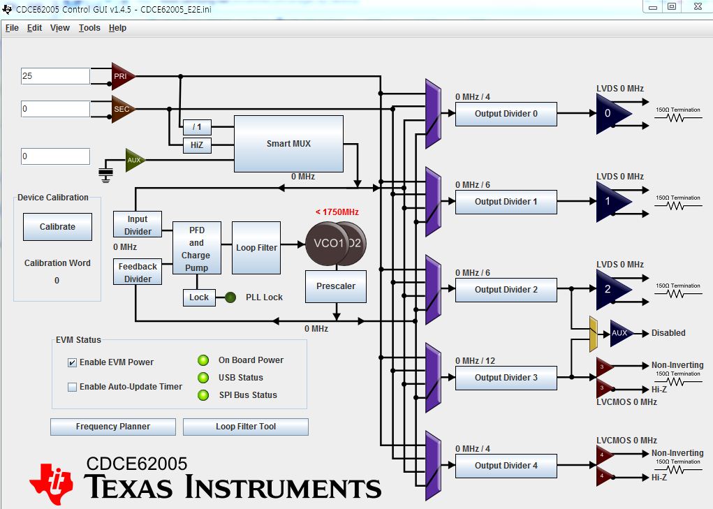
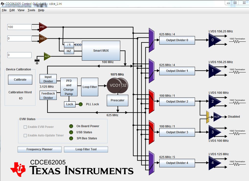
I have used the tool of CDCE62005_GUI_v1.4.5.

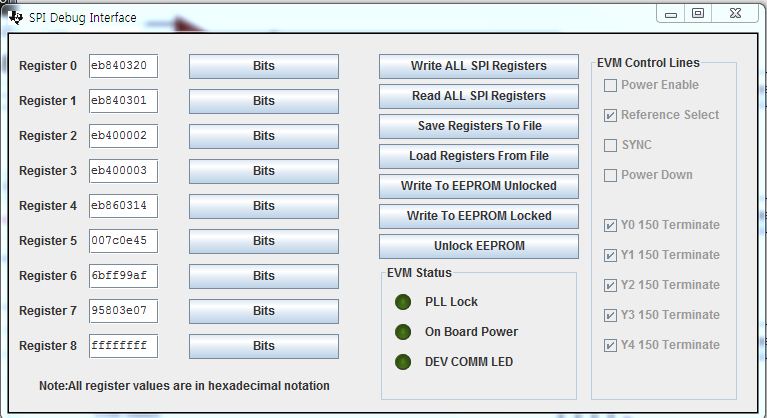
I was setting the clock rate, and get ini SPI data through SPI Debug option.

I use this data to control 62005 with SPI program of CPU.

REGISTERS
0 eb840320
1 eb03ff01
2 eb03ff02
3 210bff03
4 2185ff34
5 0024ac45
6 295f8f8f
7 bd98ad07
8 ffffffff

PORTS
0 ffffffff
1 ffffffff
2 ffffffff
3 ffffffff

INPUTS
PRI 25
SEC 0
AUX 0

EXTERNAL COMPONENTS
C4 1
R4 1
C5 1

[ Setting Value ]

1) Ref_CLK : 25MHz

2) Output port :

 - Port0 : LVDS 100MHz

 - Port1~2 : LVDS 66.667MHz (25ppm)

 - Port3 : LVCMOS 33.333MHz (25ppm, Negative port : High Z)

 - Port4 : LVCMOS 100MHz (Negative port : High Z)

3) PFD : 2.5MHz

4) Loop Bandwidth :

 - Setting Value : 250KHz

 - Phase Margin : 62.8

5) PD and LE signal : VDD rises up, SPI_LE follows VDD with 100ns and later PDn is released. 

I don't see the PLL_LOCK is high, and Clock Outputs are very unstable.

My questions below.

1) In word6, I don't know to use which value is "295f8f8f" or "295f8f86".

2) Is this setting value correct?

3) Do you have any version of GUI program?

Thank U..

  • Hi Anjun,

    let me comment on your thread. The Power Up sequence seems to be correct and by having a look at the Loop Bandwidth I assume you are using an external input (maybe LVCMOS) is this correct?

    I will have a look at the setting in order to see if they are correct.

    We are working on a new version of the GUI for Win7 operating system and it will replace the previous versions. Unfortunately it is not yet finalized and therefore is not yet released to the TI web page.

    Best regards,

    Leandro

  • Yes, Input reference clock(PRE_CLK) is LVCMOS level.

    I changed the value(get with GUI prog.) many times, but cdce62005 is not locking pll in PBA.

    I'll wait for your feedback.

    Thank u.

  •  Hi,

    could you please try the attached .ini file? I tried it out on the EVM and looks like it is locking. The bandwidth will be 237kHz and the Phase Margin roughly 60 degree. Please make sure that you have a working connection between GUI and your board.

    Regards,

    Leandro

    CDCE62005_E2E.ini
  • Thank u for your help...

    I applied the file you sent, but still PLL does not be locked.

    The other boards, developed simultaneously in same circuit, was fusing-done to use the data that is sent to a representative of your company.

    Also, They used the same method to use CPU SPI program. (we does not use cdce-Emulator.)

    Therefore, do not seem CPU SPI program issues.

    So, I'll check constantly what to do?

    Plz, I need your advise...
    cdce's power and input clock of 25MHz LVCMOS Osc. is Normal.

    And.. does register8 data must be write cdce62005 by SPI?

    The LSB of register6 is 'f', I think change 'f' to '6'. Is it wrong?

    Thank u.

  • I did test to use your ini file with CDCE_Emulator, but didn't write registers.

    When I read cdce register through Emulator, all values are "ffffffff".

    What's problem?

    thank u.

  • Hi Hanjun,

    could you please check that the Smart MUX has the PRI_REF selected?

    Also the v1.4.5 is not designed to work in a Win7 environment. The version for Win 7 is not yet officially released to the TI webpage.

    Please contact TI FAE or Sales representative for your account for further information.

    Best regards,

    Leandro

  • Hello, Leandro

    The board, that I've developed has two CDCE62005 devices.

    You help me the configuration of first one, and now, this is another configuration below.

    Through SPI configuration without Emulator, second device is not locking pll.

    Could you check that configuration?

    And, our company's TI FAE absent in our country.

    Plz, help me..

    Thank u.

    In addition, Does it must be re-writed 27th bit(ENCAL_MODE-> Manual mode) and 22th bit(ENCAL) of register6?

    PLL will not be worked after SPI write only and  PD is enable.

  • Hello Hanjun,

    please try out following settings:

    REGISTERS
    0    eb840320
    1    eb840301
    2    eb400002
    3    eb400003
    4    eb860334
    5    803c2e45
    6    2ce09a6
    7    fd90fba7
    8    200099f8

    I got the lock condition, but you may need to tune the setting for the loop filter to achieve the best performance out of your input clock.

    If you have ENCAL_MODE=0, there is no need to write the ENCAL.

    The right power up sequence is Power ON - SPI_LE high - PD enabled. You can start to write the SPI only after PD is enabled.

    I hope this can help

    Regards,

    Leandro