This thread has been locked.

If you have a related question, please click the "Ask a related question" button in the top right corner. The newly created question will be automatically linked to this question.

CDCM7005's output frequency

Other Parts Discussed in Thread: CDCM7005

From the datasheet of the CDCM7005, I have some qustions i can not understand.

The dadasheet said that ''TheCDCM7005is ahigh-performance,low phasenoise and low skew clock synchronizer that synchronizesa VCXO(voltage controlledcrystal oscillator)or VCO(voltage controlledoscillator)frequency to one of the two reference clocks.The programmable pre-divider M and the feedback-dividers N and P give a high flexibility to the frequency ratio ofthe reference clock to VC(X)O: • VC(X)O_IN/ PRI_REF=(N xP)/ M  or • VC(X)O_IN/ SEC_REF=(N xP)/ M VC(X)O_IN clock operates up to 2.2GHz.Through the selection of external VC(X)O and  loop filter components, the PLL loop bandwidth and damping factor can be adjust to meet different system requirements.''

1.How to calculate the output frequency of the CDCM7005 ?  How much the maximum  output frequency ?

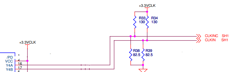
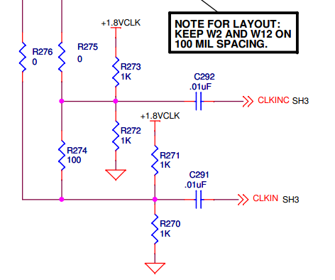
2.If  i do not provide the clock to the  VC(X)O, VC(X)O_IN (pins E1,D1) ,can the chip work normally ?  (from the DAC5670_EVM)

3.Do  the P divider supply the function of phase shift and the divider function which is simliar to the M divider ?

  • Hi Lei,

    1.the output frequency is given by the VC(X)O frequency divided by the Pdiv output which is passed through the Yx_MUX. The relationships you mentioned, are needed to configure the divider values for a correct operation of the PLL.

    2. no, the device will not work

    3. Yes, the P and M divider are very similar except for their division values.

    Regards,

    Leandro

  • Hi Leandro,

    Thanks for your reply!

    ''According to the formula : VC(X)O_IN/ PRI_REF=(N xP)/ M .If the values of the  PRI_REF、M、N、P are fixed. The frequency of the VC(X)O  is automatically adjusted to the  VC(X)O_IN=PRI_REF*(N xP)/ M ,is it right?

    The datasheet said that "The frequency applied to the Divider N must be smallert han 300MHz.A sufficient P Divider must be selected with the FB_MUX to maintain this criteria." Is it mean that the frequency applied to the Divider N is equaled to the VC(X)O_IN/ (FB_MUX  x P) ,and the frequency must be smallert han 300MHz? Is it right ?

    What is the value of the jitter of the  output frequency?


    Regards,

    Lei

  • Lei,

    this device needs an external VC(X)O. You can choose the frequency of the VC(X)O based on your output clock, but this frequency is fixed and can change of some ppm around the nominal value, based on the VC(X)O pulling range.You need to select N, P and M in order to fulfill the relationship VC(X)O_IN=PRI_REF*(N xP)/ M.

    About your second question: the signal at the FB_MUX output should be smaller that 300MHz and therefore you should select the P Divider which gives you VC(X)O/P <300MHz.

    In the datasheet you can find some value of the rms jitter like in Figure 26.

    Regards,

    Leandro

  • Hi Leandro,

    Thanks for your reply!

    About the schematic of DAC5670_EVM , i have some questions i can not understand ! From the datasheet of DAC5670_sp , i found that the input clock (DACCLK_P/N) of DAC5670 is compatibal LVPECL. But when the CDCM7005's output clock is LVPECL ,why another net is added between input of the DAC5670 and output of CDCM7005 (From the DAC5670_EVM)? Can i delete the net ? The net is followed:

    Regards, Lei