This thread has been locked.

If you have a related question, please click the "Ask a related question" button in the top right corner. The newly created question will be automatically linked to this question.

CDCE62002 can not lock to input

Other Parts Discussed in Thread: CDCE62002

Hi

I am using CDCE62002 as a clock cleaner for SERDES recovered clock.

I am halted with it more than two weeks and need some urgent help.

There are my parameters below:

----------------------------------------------

Input clock is 148.5 MHz and the output also should be 148.5 MHz.

I've built the configuration as follow:

Reference Divider = 1

Input Divider = 4

Prescaler Divider = 2

Feedback Divider = 24

VCO freq = 1782 MHz

---------------------------------

There is my CDCE62002 registers sequence by FPGA (all 32-bit registers include the register address at low nibble and sent by lsb first):

----------------------------------------------------------------------------------------------------------------------------------------------------------------

1). Write REG0=0x10360250  (LVDS REF_IN input, LVDS Output 0, Output 1 is disabled)

2). Write REG1=0x9382E061 (Loop filter settings = "0100" - External).

3). Write REG2=0x01021802 (Set PLLRST bit).

4). Write REG2=0x00021802 (Clear PLLRST bit).

5). Write REG2=0x01021802 (Set PLLRST bit, to complete 1-0-1 sequence on PLLRST and enter to the VCO CAL mode).

Unfortunately we did not purchase the evaluation module of CDCE62002 in advance, but now we would like to proceed as fast as possible with the project.

Sincerely Yours.

Boris Barak


  • Hello Boris,

    can you please provide your loop filter components to check loopbandwidth and Phase margin.

    best regards,

    Julian

  • Hello Julian,

    I have tried to operate CDCE62002 with either internal loop filter or external one.

    For the internal loop filter I have applied parameter  LFRCSEL="0011".

    For the external loop filter I have applied LFRCSEL="0100".

    I've increased the filter external components in the attempts to reach the lock as follow:

    C1 = 470 nF

    C2 = 47 uF

    R2 = 10 OHm

    CDCE62002 is never locked with the conditions above.

    Thank you very much to help me.

    Best Regards.

    Boris Barak.

  • Hello Boris,

    this settings looks fine. But please try it with LRFCSEL=1011.

    You selected LVDS as input signal with AC termination and disabled input buffer termination. Please ensure that you have the AC coupling caps and a 100Ohm resistor (between p and n) next to the input.

    Best regards,

    Julian

  • Hello Julian,

    I confirm the AC coupling caps and a 100Ohm resistor next to the CDCE62002 input on the board.

    Actually I see fo=148.5MHz on the output, but not locked to the input fi=148.5MHz and also PLL_LOCK=LOW.

    I have tried also LRFCSEL=1011, as you suggest.

    I also have some doubts regarding the CDCE62002 init sequence.

    I've implemented 1-0-1 sequence on PLLRST bit to enter into the VCO CAL mode after REG0 and REG1 setting apply.

    The question is when CDCE62002 VCO calibration will be done.

    Should I clear the PLLRST at the end of the above sequence?

    Best Regards.

    Boris Barak.


  • Hello Julian,

    I still did not advance with CDCE62002 and I don't know how to proceed.

    Can you please help me with this issue?

    Best regards.

    Boris Barak.

  • Hello Boris,

    i have build up a board with the  same loopfilter and I was able to lock the PLL properly.

    I have used this sequence:

    1). Write REG0=0x10360250 

    2). Write REG1=0x9382E061

    3). Write REG2=0x61003bf2 (Set PLLRST bit).

    4). Write REG2=0x60003bf2 (Clear PLLRST bit).

    5). Write REG2=0x61003bf2 (Set PLLRST bit, to complete 1-0-1 sequence on PLLRST and enter to the VCO CAL mode).

    Please try your board with this configuration.

    best regards,

    Julian

  • Hello Julian,

    I've tried the above sequence, but unfortunately it did not help, there is no any frequency is observed on output.

    I've tried also to use REG2=0x61023bf2 and REG2=0x60023bf2 settings for "Set PLLRST bit" and "Clear PLLRST bit" operations accordingly.

    The CDCE62002 still did not lock.

    Can you suggest some other tests in order to proceed?

    Have a good weekend.

    Boris Barak.


  • Hello Boris,

    sorry for the long delay.

    we have measured the lock condition in the lab again and recognized that you should change the loopfilter:

    C1 = 470 nF  220nF

    C2 = 47 uF

    R2 = 10 OHm

    This modification will give you more phase margin, which allows the PLL to lock with your register settings:

    REG2=0x61023bf2 and REG2=0x60023bf2 (setting CAL_bit and toggling PLL_RESET bit)

    Otherwise you could use the settings that i have sent and toggle /PD bit (register2 bit 7).

    Best regards,

    Julian

  • Hello Julian,

    Thank you very much for the efforts you apply to help me.

    I've changed the C1 capacitor value to 220nF and did the test.

    CDCE62002 outputs the designed frequency (148.5 MHz), after the registers set downloaded according to the above sequence.

    But PLL_LOCK pin is still low, indicating that output is not locked to the input.

    How can I calibrate the loop filter , trying to achieve  more phase margin to lock the PLL.

    Which other steps can be taken into account.

    I've set Lock detect Window (LOCKW="11") to the maximum value.

    Is it correct.


    Best Regards.

    Boris Barak.

  • Hello Boris,

    we finally found the issue. The input buffer termination is disabled and you are AC coupling your signal. Now the signal does not see any bias, which means that the signal has no DC component.

    By enabling the input buffer termination (reg 0 bit 5 = 0)  the input gets biased with 1.2 V. After that you should get the lock condition.

    please try these writing sequence:

    1). Write REG0=0x10360050  (LVDS REF_IN input, LVDS Output 0, Output 1 is disabled, input buffer termination enabled.)

    2). Write REG1=0x9382E061 (Loop filter settings = "0100" - External).

    3). Write REG2=0x01021802 (Set PLLRST bit).

    4). Write REG2=0x00021802 (Clear PLLRST bit).

    5). Write REG2=0x01021802 (Set PLLRST bit, to complete 1-0-1 sequence on PLLRST and enter to the VCO CAL mode).


    Best regards,

    Julian

  • Hello Julian,

    I've did the suggested sequence and CDCE62002 was locked indeed to the input.

    But sometimes while sampling PLL_LOCK the frequency oscillation can be seen, meaning that CDCE62002 sometimes loose the lock (see attached).

    I've tested it either with 100 Ohm resistor (between p and n) next to the input or without it (do you recommend to remove this resistor while enabling the input buffer termination?).

    Please see below the PLL_LOCK pin sampled by scope while not locked and input vs. output frequency waveforms, while locked (Fin is on CH1 of the scope).

    6052.PLL_LOCKpinOSC.TIF

    7840.Fin(CH1)vsFout(CH2)_148.5MHz.TIF

    Best Regards.

    Boris Barak.

  • Hello,

    There is a long time since I've put the last post related to CDCE62002 here.

    We've just discovered some defect with the product, related to CDCE62002 chip.

    CDCE62002 PLL chip is not fully locked, but is going from "lock" to "out of lock" , when trying to boot it when hot (about ~50° on chip body).

    Need urgent help on this issue.

    Please see attached snapshot below.

    CDCE62002_PLL_LOCKpinOSC.TIF

     Best Regards.

    Boris Barak.

  • Hello Boris,
    Do you see this behavior on the EVM?
    Would you please send the full device configuration as well as details about the input source.
    Regards,
    Ahmed
  • Hello Ahmed,

    Thank you for your answer.

    I don't have the evaluation board, but only the data sheet of it.

    I keep the same calibration sequence, as suggested earlier in this thread (REF=148.5MHz, U0=148.5MHz).

    1). Write REG0=0x10360050  (LVDS REF_IN input, LVDS Output 0, Output 1 is disabled, input buffer termination enabled.)

    2). Write REG1=0x9382E061 (Loop filter settings = "0100" - External).

    3). Write REG2=0x01021802 (Set PLLRST bit).

    4). Write REG2=0x00021802 (Clear PLLRST bit).

    5). Write REG2=0x01021802 (Set PLLRST bit, to complete 1-0-1 sequence on PLLRST and enter to the VCO CAL mode).

    I've tried a different settings of the external loop Filter.

    Please see the CDCE62002 lock pin snapshot for 1kHz and 10kHz external filter settings, cold_start__CDCE62002_1kHz_lock_pin.TIFcold_start__CDCE62002_10kHz_lock_pin.TIFhot_start__CDCE62002_1kHz_lock_pin.TIFhot_start__CDCE62002_10kHz_lock_pin.TIF

  • Hello Boris,
    The loss of lock points to incomplete or erroneous VCO calibration.
    would you please try the following ..
    - repeat steps 3 to 5 just to confirm it's related to calibration
    - try the PD sequence to trigger the calibration. i.e. change the 3-5 steps to
    3. Write REG2=0x01001802 (set CAL to PD)
    4. Write REG2=0x01001002 (PD = 0)
    5. Write REG2=0x01001802 (PD= 1, CAL should be triggered)
    Please let me know if you see any change.
    Regards,
    Ahmed
  • Hello Ahmed,

    I did the changes according to your recommendation (please verify the calibration sequence below).

    It looks better.

    Should also be verified by QA team on few units.

    Here is updated CDCE62002 calibration sequence:

    (REFin=148.5MHz, U0=148.5MHz).

    1). Write REG0=0x10360050  (LVDS REF_IN input, LVDS Output 0, Output 1 is disabled, input buffer termination enabled.)

    2). Write REG1=0x9382E061 (Set PLL dividers, Loop filter settings = "0100" - External).

    3). Copy RAM (REG0 and REG1) to EEPROM command – write 0x0000001F.

    4). Delay - to ensure stable copy command.

    3). Write REG2=0x01001802 (Set #PD bit to '1')

    4). Write REG2=0x01001002 (Set #PD bit to '0', CDCE62002 power down by #PD 1-to-0 transition)

    5). Write REG2=0x01001802 (Set #PD bit to '1', to complete 1-0-1 sequence on #PD and enter to the VCO CAL mode).

    best Regards.

    Boris Barak.

  • This looks fine, Please let us know if the issue appeared on other units. in such failure of calibration, repetition of the cal sequence with some delay might help in some cases.
  • Hello Ahmed,

    We did a complete test of the few units in the thermal chamber (0°C - 45°C).
    The above temperature values are related to environment and not to the chip temperature.
    The results are pretty good.
    However, sometimes CDCE62002 did not lock at low temperatures (random), 0°C-10°C.
    I am wondering if there are some possibilities to make an additional improvement to the calibration flow.
    On the other hand the jitter performance is still little higher than required.
    Can you give any tip to improve it?

    With Best regards.
    Boris Barak.
  • Hello Boris,

    Going back through the thread, I noticed you changed your external LF setting to "0100", are you still using the external components as before?

    C1 = 470 nF  or 220nF, C2 = 47 uF, R2 = 10 OHm

    In that case your phase margin might be on the critical side, it's around 52-57 degrees. given that you are starting at corner tempratures, I would highly recommend to increase this phase margin for reliable locking, make sure it's above 70 degrees to have enough margin on the temp corners.

    you can use the CDCE62002 GUI loop filter tool to predict the phase margin as in the picture attached.

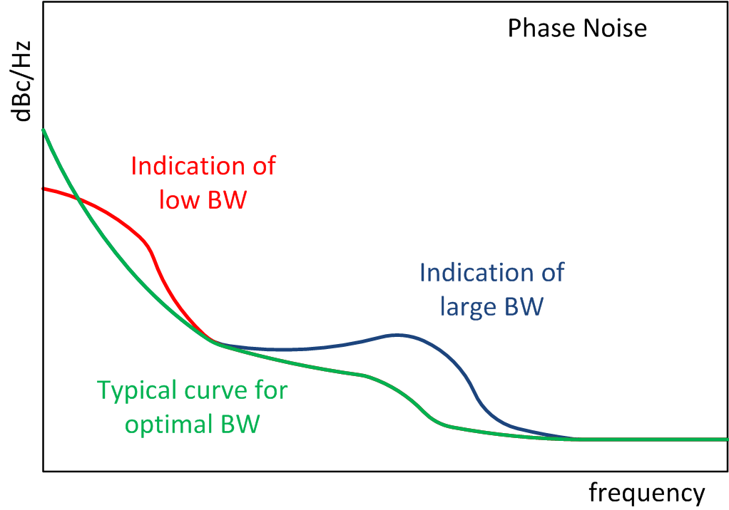
    Regarding jitter performance, the optimum performance is achieved when the loop bandwidth is set such that the open loop contribution of the VCO and the reference source phase noise contribution are balanced. if you know you have a noisy reference source, then you might need to tighten your loop-bandwidth (maintaining enough phase margin).

    one easy way to see if you have the proper BW is to monitor the output phase spectral density on a phase noise analyzer like Agilent E5052A, a hump in the phase noise plot is an indication of too large BW, a high close-in noise level is an indication of a narrow BW.

  • Hello Ahmed,

    Thank you.

    Here is the snapshot of the exact current CDCE62002 configuration in the board.

    What do you think about?

    I will check if we can do some measurements with noise analyzer after the weekend.

    Best Regards.

    Boris Barak.

  • Hi Boris,
    Your phase margin sounds good. is the failure to lock happens to the same chips randomly? or can happen to any chip?
    Is the reference input available at the time of reset? or the reference itself goes through reset?
    The calibration process requires a stable input. it works better with lower PFD frequencies, so this is something you might try to lower fPFD.
    Please also try to repeat the PD/PU for triggering the calibration in case of calibration failure after some time delay.
    Ahmed