This thread has been locked.

If you have a related question, please click the "Ask a related question" button in the top right corner. The newly created question will be automatically linked to this question.

CDCE62005 PLL Lock problem

Other Parts Discussed in Thread: CDCE62005

Hi,

We have designed a board with two C6678 DSPs and we use two CDCE62005 clock generators.

Each clock generator has a separate 25MHz external oscillator.

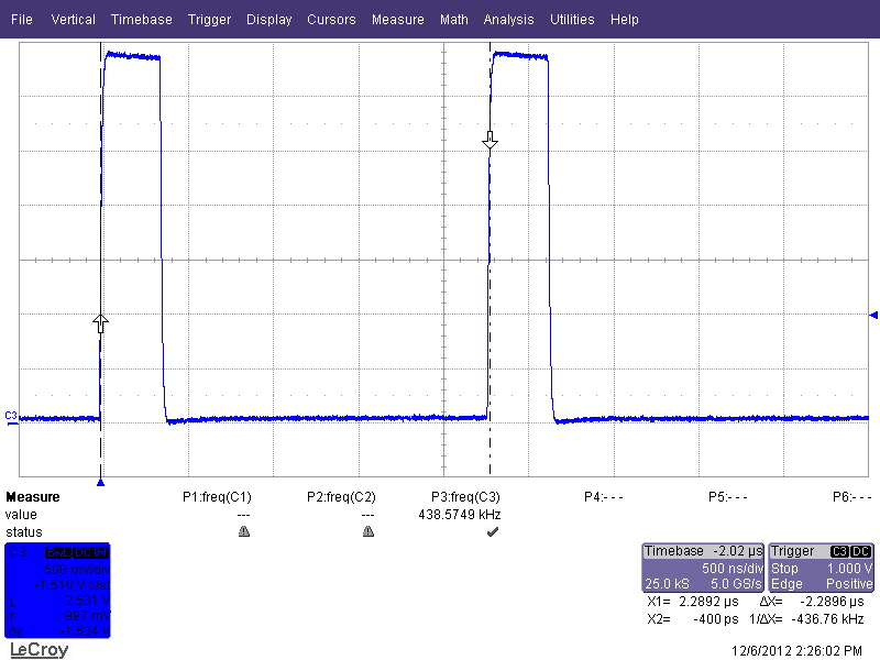
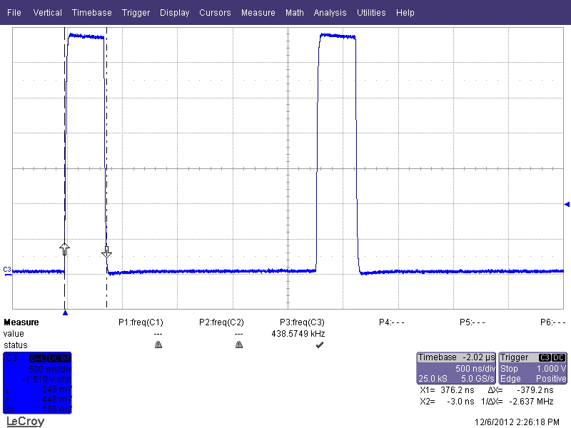
The problem is that both devices does not have PLL lock. This signal toggles but id does not achieve PLL lock.

CLK1 has one output of 100MHz and four outputs of 250MHz (all outputs are LVDS).

CLK2 has all five outputs of 100MHz (all outputs are LVDS).

Here are the registers:

CLK1:

0    e9 85 ff 20
1    e9 85 ff 21
2    e9 07 ff 02
3    e9 85 ff 03
4    e9 85 ff 14
5    10 00 0b 35
6    00 fe 03 e6   // Reg. 6 bit 27 is '0' for start-up PLL calibration mode
7    fd ff ff f7

CLK2:

0    e9 07 ff 20
1    e9 07 ff 21
2    e9 07 ff 02
3    e9 07 ff 03
4    e9 07 ff 14
5    10 00 0b 35
6    00 fe 03 e6   // Reg. 6 bit 27 is '0' for start-up PLL calibration mode
7    fd ff ff f7

Please advise!

  • Hi,

    I looked at your registersand you didn`t select a valid loopfilter the phase margin is about 90deg or more, this will case a not stable Loop.
    Therefore, please try these register settings. The loopfilter is adjusted to 54deg phasemargin. The remaining settings are the same.


    CLK1:
    0  e9 85 ff 20
    1  e9 85 ff 21
    2  e9 07 ff 02
    3  e9 85 ff 03
    4  e9 85 ff 14
    5  10 00 0b 35
    6  00 6e 03 e6
    7  bd a2 3d f7

    CLK2:
    0    e9 07 ff 20

    1    e9 07 ff 21
    2    e9 07 ff 02
    3    e9 07 ff 03
    4    e9 07 ff 14
    5    10 00 0b 35
    6    00 6e 03 e6  
    7    bd a2 3d f7

    best regards
    Michael

  • Hi Michael,


    Thank you for your reply!

    Yes you are right. I have already realized this problem. We changed to the following settings and it's working now:

    CLK1:

    0          e9 85 ff 20

    1          e9 85 ff 21

    2          e9 07 ff 02

    3          e9 85 ff 03

    4          e9 85 ff 14

    5          10 00 0b 35

    6          00 3F 03 e6

    7          BD A1 7b E7

    Phase margin: 63.8 deg

    Loop bandwidth: 242 KHz


    CLK2:

    0          e9 07 ff 20

    1          e9 07 ff 21

    2          e9 07 ff 02

    3          e9 07 ff 03

    4          e9 07 ff 14

    5          10 00 0b 35

    6          00 2F 03 e6 

    7          BD A1 79 E7

    Phase margin: 61.9 deg

    Loop bandwidth: 256 KHz


    Is the 54 deg phase margin a better choice?

    Thank you for your help!


  • Hi,

    phase margin between 60 and 65 is perfect (usual between 45 and 70deg).
    The bandwidth is ~1/10 of the VCO freq, this is also very good.

    best regards

    Michael

  • Hi,


    After extensive testing of the PLL, we notice that it locks sometimes but in most cases the PLL does not lock.

    The signal of the PLL_Lock "jitters" Indefinitely. Attached are scope captures of the PLL_Lock signal.

    The PLL settings are as follows:

    0          e9 07 ff 20

    1          e9 07 ff 21

    2          e9 07 ff 02

    3          e9 07 ff 03

    4          e9 07 ff 14

    5          10 00 0b 35

    6          00 2F 03 e6  

    7          BD A1 79 E7

    We checked voltages are good and the 25MHz crystal is working.

    Please advice!


  • Hi,

    can you tell, do you trigger by the time the device is starting up or after several seconds?
    Because the calibration and lock  takes a time, it`s depending on the input clock and loopbandwidth.If  you need -> CDCE62005 on page 67/68 you`ll  find detailed information about start up and calibration times.
    The locksignal should be High for lock.

    Best Regards
    Michael