


Other Parts Discussed in Thread: LMX2541, LMX2531
Hi,
my customer designs a clock generation module on LMX2541 pin compatible with the module based on ADF4106. This is done to avoid VCO tuning.
However, the startup waveforms of the two circuits are different. LMX 2541 requires that signals Data, Clk, LE are to be set to "0" after loading. For ADF4106 buffer is used, that blocks the activity of the common SPI bus with the help of signal LE:
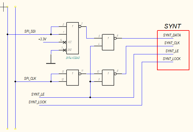
In this circuit, the signal LE is "0" only during synthesizer loading, and the rest of the operation it is in the state "1", thus blocking the activity of the signals CLK and SDI. The loading diagram of ADF4106 uses a lower version of the LE signal behavior:

Since the customer is using the "full chip" mode of LMX2541, the calibration process of internal VCO starts after loading the final register R0. In order not to interfere with this process, the signal LE must not be kept in a state of "1" for more than 1 us (Tewh).

The customer asks to clarify why it’s needed to keep the signals Data, Clk, LE in the state "0" if a normal shift register is used and the counter is updated on rising edge of LE? What happens on the last falling edge of LE at the end of startup process? What happens if I do not lower the LE signal to "0"?


