Other Parts Discussed in Thread: LMK03806, CODELOADER
We use a LMK03806 Clock IC and are not able to interface the LMK with our onboard microcontroller SPI Peripheral. There was also a SoftwareSPI at hand (Manual pin toggling) which was able to configure the LMK finally.
But it is still unclear why the Hardware SPI Solution does not work, because the Timing requirements stated in the datasheet look fullfilled.
All testruns contain the same bytesequence (except 16bit zero on start for Hardware SPI without LatchEnable!)
Find more details below,
Best regards. andreas
HW Setup:
- LMK03806 [2]
- STM32 Board (ARM Cortex M4) [1]
- Connection directly, no buffers
- For all Firmware tests, the Hardware setup stayed the same (including PIN's)
Osci Setup
|
Channel |
Data |
|
A |
Readback |
|
B |
MOSI DATAuWire |
|
C |
SCK |
|
D |
LatchEnable LE |
SPI Setup:
In General following Setup is used (noted otherwise)
SCK Default Low, Input valid on Rising Edge.
Byte Sequence:
The generated Code Sequence was generated via Ti CodeLoader 4.6.1 .
The Sequence is starting with 0x80020140. Full sequence can be found at bottom.
Several Firmware Options were tested:
Software SPI - working
SPI is implemented using manual Pin Toggling in Software.
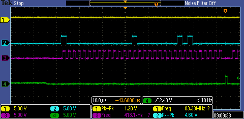
[FIGURE 7 - SW SPI - Full View on init Data 0x80020140]

[Figure8 - SW SPI - Zoom on first Bit]
Here the LMK is working as expected (readback was not tested)- clock's are as required on their outputs & Pin 33 goes to High after finishing.
Trigger is set here on LatchEnable.
Hardware SPI - not working
Here, before the 0x80020140 sequence was started, 16 empty bits are clocked out to clear all buffers.
There was also a test without the first 16 zero bits, same result.

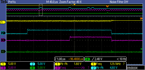
[FIGURE 5 - HW SPI - Full View on init Data 0x80020140]
[Figure6 - HW SPI - Zoom on first Bit]
It can be seen here, that the bit setup is done on falling edge, and read in can be done on rising edge.
Trigger is set here on LatchEnable, already armed when uC program started running. So no LatchEnable happens before this point in time.
Hardware SPI - not working too, but strange result
Here, the SPI Settings were changed from firstEdge to secondEdge. I know that this setup should not work in general, but it was just a try because nothing else worked either.
The LMK now responds after finishing the programming sequence with enabling Pin 33 to High. But the Output Clocks are not correct. This Test was just done to

[FIGURE 3 - SW SPI - Full View on init Data 0x80020140]
Programming Sequence:
0x00000f00,
0x00000F01,
0x00000F02,
0x00000f03,
0x00000f04,
0x00000965,
0x0CC80006,
0x0C0C0007,
0x080C0008,
0x55555549,
0x9C02400A,
0x3400102B,
0x138C006C,
0x3D03826D,
0x0300000E,
0xC1550410,
0x00000018,
0x8FA8001A,
0x0010001C,
0x018000DD,
0x040000DE,
0x001F001F
References
[1] http://www.st.com/st-web-ui/static/active/en/resource/technical/document/user_manual/DM00039084.pdf
[2] http://www.ti.com/lit/ds/symlink/lmk03806.pdf