Other Parts Discussed in Thread: CDCE62005, LMK00105
Hello Sir,
I am Vijetha H.N, Hardware Design Engineer at iWave Systems, Bangalore, India.
We are designing a PCB using CDCE62005 as the clock synthesizer. I have some queries related to the design using CDCE62005.
Design Decsription :
The design includes FPGA (Stratix V, ALTERA) and CDCE62005 is used to provide REFCLK (Thransceiver Referance clock) to FPGA. The SPI interface to Synthesizer is derived from CPLD (Max V, ALTERA).
The Clock Design Flow:
50 MHz Oscillator -> 1:5 LVCMOS Clock Repeater (LMK00105SQE/NOPB) ->Sec_Ref pin of Clock Synthesizer(CDCE62005) -> 1:4 LVDS Clock Repeater (CDCLVD1204RGTT) -> REFCLK pins of FPGA (Stratix V, ALTERA).

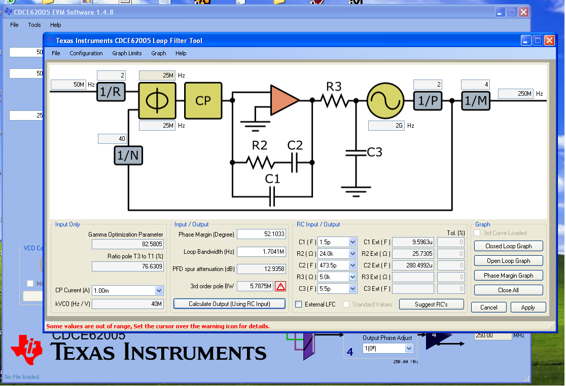
Input Spec for CDCE62005 = 50 MHz LVCMOS (to Sec_Ref).
CDCE62005 Output Requirement = 250 MHz LVDS on 5 outputs.
REFCLK Phase noise requirement for FPGA = -120 dBc/Hz
REFCLK Phase Jitter requirement for FPGA = 1.2 ps.
I am new to the design of clock synthesizer, so I request you to guide me by answering the below queries.
1. What should be the Bandwidth of the loop filter for the above requirements?
2. Please mention the required factors to be considered and standard procedure to be followed to select/calculate the Bandwidth of the PLL, so that 250 MHz clock is generated without noise/jitter.
Thank You,
Regards,
Vijetha H.N