Other Parts Discussed in Thread: CDCLVC1104
Hi,
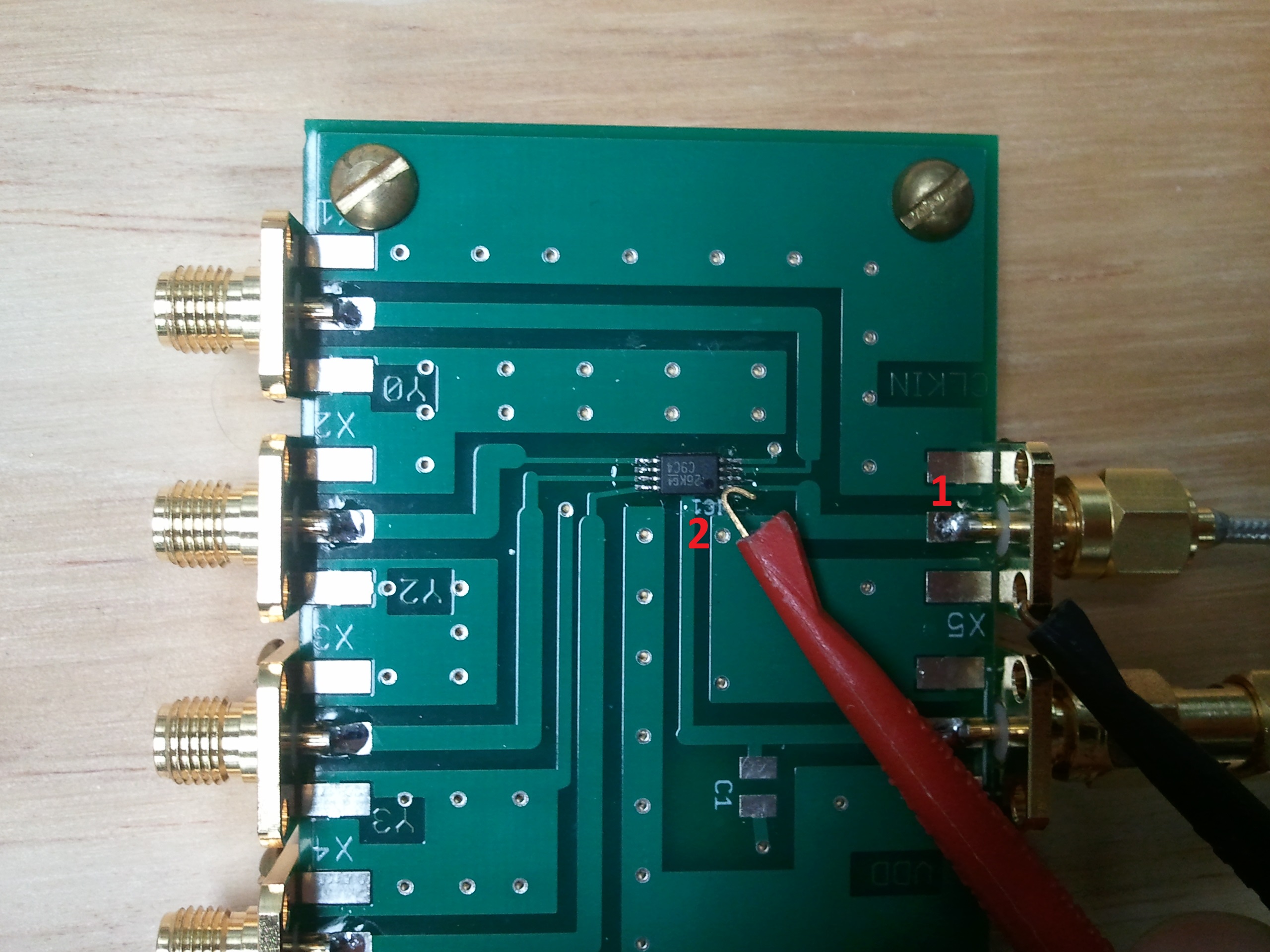
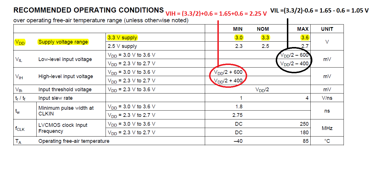
I have the 1:4 Clock Buffer chip: CDCLVC1104. The questions I have are as below:
1) What kind of input signal (pin 1) does this buffer chip accepts i.e.: Sinusoidal, pulse or both ?
2) Does the input signal has a upper power bound (max. power input signal can have on pin 1) ?
3) What voltage signal shall I use for enable pin for the chip (pin2) ?
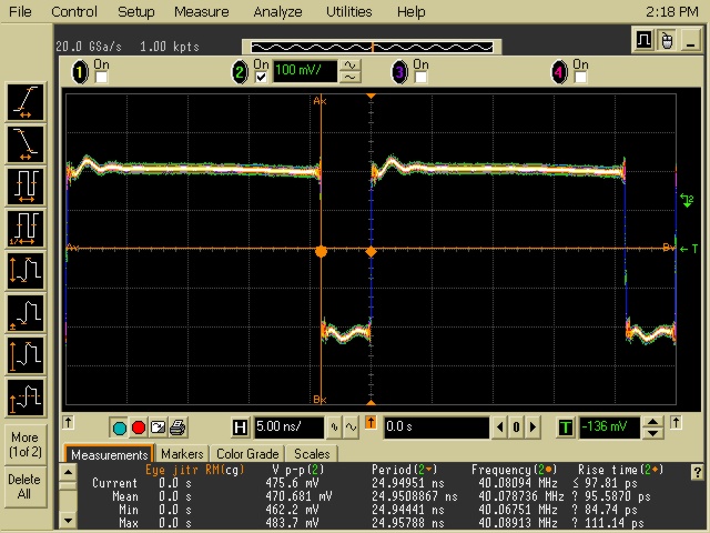
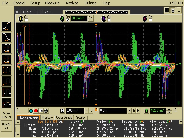
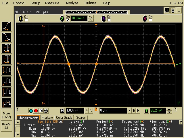
4) Datasheet claims fmax=250 MHz at 3.3 V. But I get a clean sine output (when input is a sine wave) for higher frequencies than this fmax. Matter of fact when I input the lower frequencies (i.e. 40 MHz) the output signal is distorted.
link to find the CDCLVC1104 datasheet: http://www.ti.com/product/cdclvc1104
Thank you in advance.
Regards,
Valay Shah