This thread has been locked.

If you have a related question, please click the "Ask a related question" button in the top right corner. The newly created question will be automatically linked to this question.

Drive Capability of MISO pin of CDCE62005

Other Parts Discussed in Thread: CDCE62005

Hello Sir,

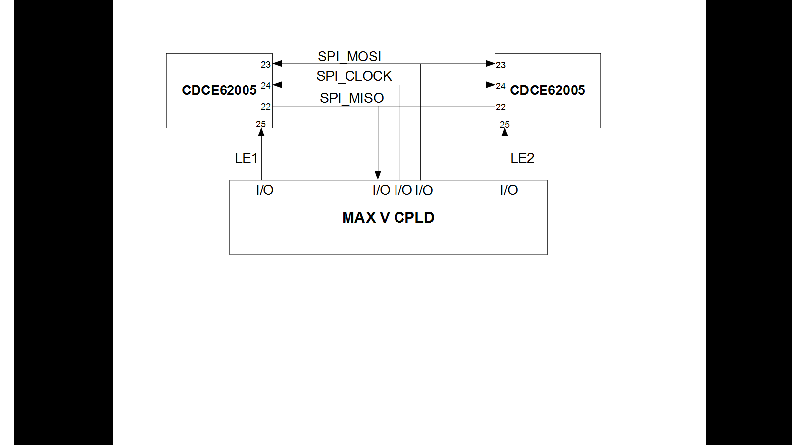
We are using 2nos of clock synthesizer IC CDCE62005 in our design. The SPI interface signals are connected to MAX V CPLD I/O pins as shown in the image

My Query :

In the datasheet of CDCE62005, it is mentioned that the typical output load capacitance value for MISO is 3 pF. The CPLD I/O pins have input capacitance of 5 pF. Is this value 3 pF a typo error? 

And in my design, the MISO of both ICs drive same I/O. Is there any issue in this type of connection, in spite of these capacitance value mis match ? (NOTE : I have provided Pull up for the MISO at the CPLD side).

Please clarify on this.

Regards,

Vijetha

  • Hello Vijetha,

    it is possible to connect the 2 CDCE62005 in this way.

    The 3 pF output capacitance is correct as well. That just means that the open collector output is connected to 3pF + 5pF (Co of CDCE62005 and Ci of CPLD).

    best regards,

    Julian

  • Hi Julian,

    Thank you for the information. A small clarification needed.

    As per my understanding usually the output and input load capacitance is given to check the driving capabilities. We usually expect the output load capacitance of driver to be more than the input capacitance of the receiver (so that the drive current will be more than the expected/required receiver current). In the above design, this condition was not meeting, hence I got this doubt. I just wanted to know whether my understanding of the load capacitance (explained above) is correct and if it is correct then how this mismatch does not cause the issue? 

    Regards,

    Vijetha

  • Hi Sir,

    I have understood this point.

    We will look into the rise time using the formula I = C * dv/dt, I = Sink current (33mA), C = 11 pF (3pF + 3 pF + 5 pF), dv = 3.3 * 80% (90%-10%). From this we get rise time and the value is compared to the rise time expected at the CPLD I/O pin.