


Hi,
We are planning to use CDCVF2505 as the reference clock(RMII REFCLK) for AM335x and ethernet PHY.
we are confused on how to connect CDCVF2505 terminals properly.
The datasheet mention's that CLKOUT can be loaded with a capacitor to adjust the input-to-output propagation delay
but we don't know what value should be connected.
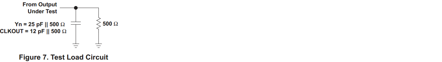
The electrical characteristics table in the datasheet mentions Output capacitance(Co) as 5.2pF(TYP)
but the "Figure 7. Test Load Circuit" on page 7(Below) shows 12pF.
Please let me know what is the best value to be choosed if we are not concerned about any delay or zero delay?
And also do we need to connect 500ohm resistor in parallel to this capacitor?
And regarding unused pins (in our case only 1Y0 & 1 are used), how to terminate the unused pins(1Y2,1Y3)
should it be left floating?
Just in case please let me know if there is any Reference design of this Clock Driver.
Regards
Prad.
