A related question is a question created from another question. When the related question is created, it will be automatically linked to the original question.
If you have a related question, please click the "Ask a related question" button in the top right corner. The newly created question will be automatically linked to this question.
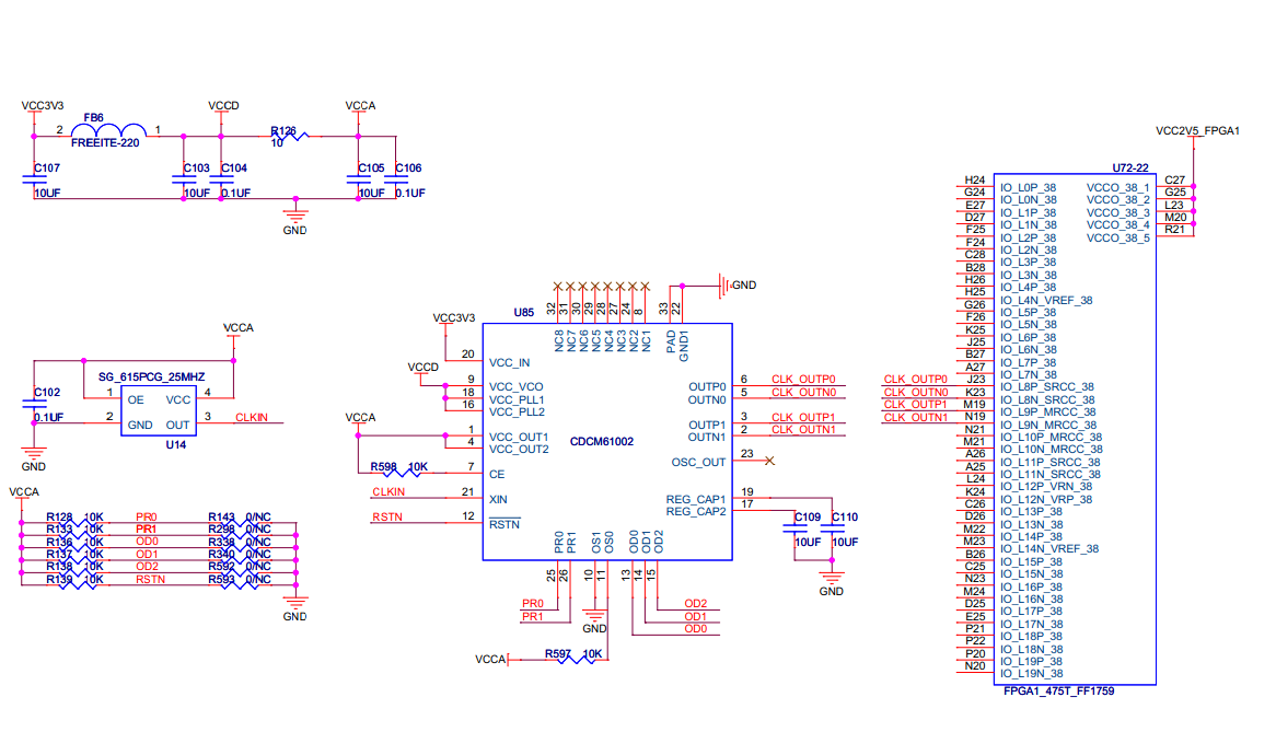
I am looking for an application circuit diagram for the CDCM61002, it is not in the datasheet. I have checked out the EVM circuit schematic but it is very blurred.
We provide a snapshot of a reference circuit using the device on page 7 of this document. In addition, the EVM User's Guide gives some additional recommendations on input and output termination, when needed. Let me know if this is what you are looking for.
1.The input level of the chip is LVCMOS(3.3V), but Virtex-6 FPGA does not this standard. Can i directly drive the control signals of the CDCM61002,for example "OD0,OD1,OD2,RSTN..." through the FPGA(Bank vcco 2.5v).
2.From the datasheet(page 25),i found that from the output of the chip to the LVDS determination,there is a 100ohm resistor ,why?when i directly connect to the FPGA,can i delete the resistor?
3.Please give some advice about my design,the picture followed: