Hi,
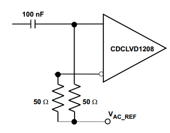
My customer want to fanout 50MHz XO output to multiple loads through CDCLVD1208. However, their 50MHz XO is 3.3V LVCMOS output, while CDCLVD1208 can only accept 2.5V LVCMOS input. How should they do? I am considering below interface ckt, could you please help me review if there is any problem with it?

The consideration of this design is to attenuate 3.3V LVCMOS XO output down to below 2.5V througn serial resistor (R2) and 49.9ohm shunt resistor (R1) to accomodate input requirement of CDCLVD1208. Meanwhile the R1 resistor also act as termiator and input bias. What I am not sure is that the AC load for XO output will be arround 100ohm, I am wondered if it will result any problem for XO due to so heavy load.
Thank you,
John