This thread has been locked.

If you have a related question, please click the "Ask a related question" button in the top right corner. The newly created question will be automatically linked to this question.

LMK04828 3 wire SPI read

Other Parts Discussed in Thread: LMK04828

Hi,

I am trying to read the registers of LMK04828 in 3 wire SPI mode and having trouble. The data sheet Figure 1 in Read mode is unclear and misleading. Do I clock in first 16 bits and then change direction of SDIO pin and clock out 8 bits of data or there should be two separate 24 bits SPI transactions: first one to clock in R/W, W1, W0, Address and 8 dummy bits of data and the second one to clock out 24 bits with only 8 LSB valid (Figure 1 looks this way). I am confused.

Thank you,

Vlad.

  • So a read can be done in a single 24 bit transaction.

    Clock R/W = 1; W1 & W0 = 0.  Address as desired.  Then flip your SDIO line for input, and then provide the next 8 clocks for data.

    I see your point about how it's confusing.... I think the intention of "SDIO (Read)" may have been to show the timing for the readback on a 4th pin.  It's incorrectly/poorly labeled.  I think will simply add more figures to clarify vs. trying to get all the info in one.

    73,

    Timothy

  • Hi Timothy,

    Thank you for the clarification . Hope it will help.

    Regards,

    Vlad.

  • hello Timothy:

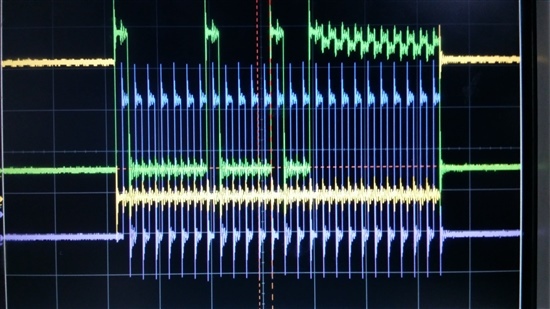
           I met a likely problems about the spi 3 wire reading.I am  using the LMK04828EVM , I want to config the lmk04828 with the outside FPGA borad  using 3 wire SPI interface. I do the  timing as you said, just like the datasheet. But it seems that  the read out data waveform  i captured by oscilloscope  is hign dependence? The captured wave form i paste below. Why there is no readback data?

    This problem has confusing me a week. Please help me, thanks! 

  • Hi Timothy,

    Do we need last 8 bits high impedance or do we need to separate this to two transactions ?

    Best regards,
    Nir.
  • Hello Nir,

    The readback should be able to be accomplished using a single transaction.  So after writing the R/W (as 1), W0/W1 (as 0), then the address, the state for your masters IO pin will change to either tri-state or pull-up.  Note that SDIO_RDBK_TYPE = 0 (pushpull) or 1 (open drain output -- requires external pull-up from PCB or master).


    To assist your debug, I suggest enabling one of the other pins for 4th wire readback so you can see the output data without the possible confusion of the master.  See attached.

    73,
    Timothy

    8787.SPI Readback on LMK04820 Family.pdf