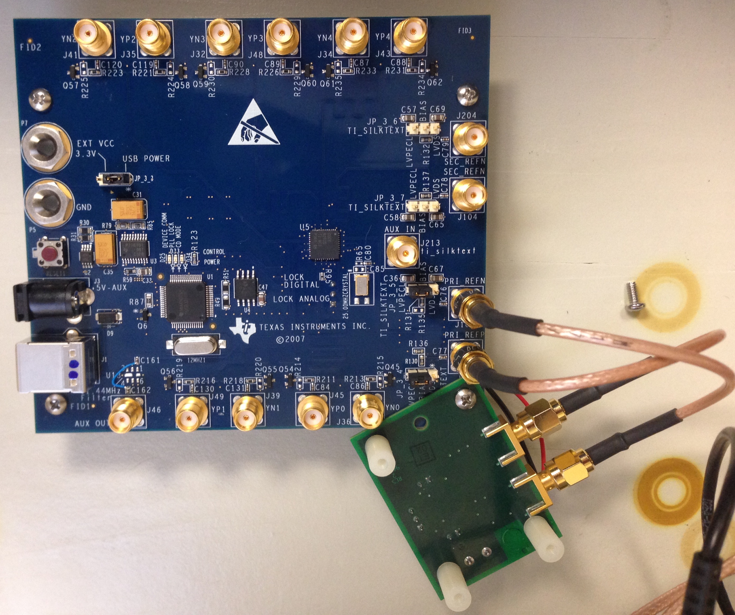
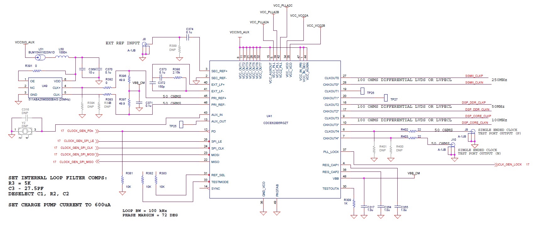
We are having an issue getting our CDCE62005 on a custom board, to lock with an LVPECL reference input. I have included the schematic below.
The datasheet for the crystal used (we are using the LVPECL variant of the part) is below
/cfs-file/__key/communityserver-discussions-components-files/48/1207.si510_2D00_11.pdf
1) We have removed R396 and R397, in favor of using the part's internal termination.
2) We initially tried the external Loop filter as shown in the schematic with the internal components set per the schematic notes. These register settings are listed in the the CDCD62005_2015_05_29 files (TPS and ini).
These values did not "lock" the PLL for us.
3) We then attempted to make an adjustment to increase the loop bandwidth( to 225KHz), and decrease the phase margin ( to 68 degrees). The files generated by the EVM software are below.
We also had to change the schematic components as follows (per recommendation of the EVM software)
- R398 = 4.7K ( was the closes value to the 4.99k the EVM software generated)
- C373 = 0.01u
- C372 = 47pF
These settings did not result in a lock either.
4) Finally we attempted injecting a 3.3V LVCMOS 10MHz square wave in J8 to (SEC_REF). The values generated by the tool, resulted in us getting an actual lock from the PLL.
Unfortunately we can't ship a signal generator with our product ;-) , so we need to figure out why we can't get the crystal input on the primary reference input to lock. Are there any suggestions, recommendations, or are there any obvious issues with our crystal input in our design?
Thanks,
Mark