This thread has been locked.

If you have a related question, please click the "Ask a related question" button in the top right corner. The newly created question will be automatically linked to this question.

LMK04821

Other Parts Discussed in Thread: LMK04821, LMK04828, LMK04000

Hello,

Here are few questions regarding LMK04821.

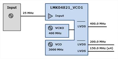
1. Following WEBENCH designer results, sometimes I need external VCXO and sometimes no (see below picture). Why?

According the device functional modes that mention in datasheet, we always need external VCXO or Tunable Crystal.

Can you explain when I need to add external VCXO? (if I don’t need the VCXO , can I connected directly the CPout1 to Loop filter circuit and then to OSCin?)


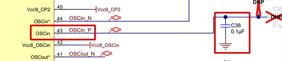
2. What is this circuit mean? Is that required for each design?  


3. According to datasheet, I need to connected the OSCINN to GND via capacitor. In the EVM pin OSCIN connected to GND via capacitor instead of OSCINN. Please advise.         

    4. On LOOPFILTER1 - The WEBENCH calculated that VCO frequency is 100MHz. Is the external VCO that I need to add to my design? If yes, do you have an application note how to select the right VCO/VCXO?


 5. On LOOPFILTER2 - The WEBENCH calculated that VCO frequency is 3000MHz. This is an internal VCO. I need to add only the EXT Loopfilter component, Right?   


Thanks,

Idan.


  • Idan A said:
    1. Following WEBENCH designer results, sometimes I need external VCXO and sometimes no (see below picture). Why?

    We have plans to improve the design of dual loop devices.  Right now the tool displays the VCXO in the block diagram if used for providing one of the unique frequencies.  However when simulating there is always an VCXO used, you will see this from the LOOPFITLER1 VCO Frequency, that is the frequency the external VCO is operating at.
    The LMK0482x (and LMK0480x) are multi-mode devices.  They can be used for dual loop, single loop, or clock distribution.  To simulate for single loop, I recommend setting a very narrow (1 Hz) loop bandwidth, this 'jitter cleaning' makes the device operate as if the VCXO input (OSCin) is the reference without any noise impacts of PLL1.

    For more info on why to select dual loop or single loop, refer to the "Choosing PLL Loop Bandwidths" on the Files section of this Clock & Timing E2E Forum.  Summary: when input is noisy, when input is low frequency, when input frequency and VCO frequency have a poor integer relationship resulting in low phase detector frequency.

    I notice you are using LMK04821 for your designs.  Is there a reason you're not using LMK04828 which can get all your frequencies from the VCO directly?

    Idan A said:
    According the device functional modes that mention in datasheet, we always need external VCXO or Tunable Crystal.
    Can you explain when I need to add external VCXO? (if I don’t need the VCXO , can I connected directly the CPout1 to Loop filter circuit and then to OSCin?)
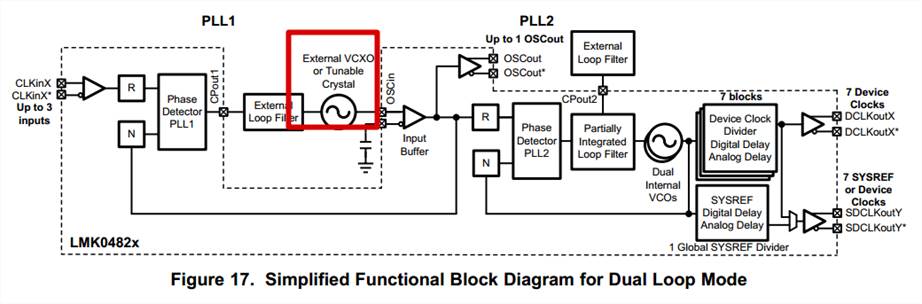
    You don't always need an external VCO/VCXO, you can connect your reference directly to OSCin and power down PLL1.

    Idan A said:
    2. What is this circuit mean? Is that required for each design?

    This is not required for each design.  This is a super set design which allow for crystal mode, VCXO, single ended, or differential VCXOs.

    General use case would be with a 3.3 V LVCMOS VCXO.  The circuit I suggest for this is 100 ohm series resistor - series DC blocking cap - transmission line - 50 ohms to ground termination (and voltage division), series DC blocking cap - IC.  On the unused pin OSCin or OSCin* place a cap to ground.

    Idan A said:
    3. According to datasheet, I need to connected the OSCINN to GND via capacitor. In the EVM pin OSCIN connected to GND via capacitor instead of OSCINN. Please advise.
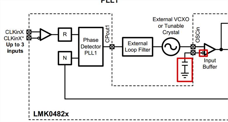
    You can use either OSCin or OSCin*, OSCin is a bit further away from other clock outputs for crosstalk considerations.  However based on the pinout of our device and differential/single ended VCXOs, it works out that OSCin* is the input we use from a single ended VCXO.

    Idan A said:
    4. On LOOPFILTER1 - The WEBENCH calculated that VCO frequency is 100MHz. Is the external VCO that I need to add to my design? If yes, do you have an application note how to select the right VCO/VCXO?
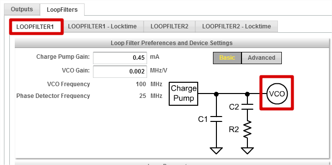
    You're correct, this is the actual VCXO frequency being used.  Consider the app note, AN-1910 LMK04000 Family Phase Noise Characterization, (snaa063).

    Note that you can enter/change the VCXO frequency on the advanced LOOPFILTER1 page, you will also need to adjust the PLL2 phase detector frequency on the LOOPFILTER2 advanced page.  Adjusting the PLL2 phase detector frequency to be 2x the VCXO frequency is a technique to simulate with the doubler, be aware that divider validity is not checked when doing this.

    Idan A said:
    5. On LOOPFILTER2 - The WEBENCH calculated that VCO frequency is 3000MHz. This is an internal VCO. I need to add only the EXT Loopfilter component, Right?

    Correct: C1, C2, and R2.

    73,
    Timothy