This thread has been locked.

If you have a related question, please click the "Ask a related question" button in the top right corner. The newly created question will be automatically linked to this question.

URGENT, LMK04828 clock output frequency isn't correct. Hi Timothy, if you see this post, please take a look at my questions, thank you!

Other Parts Discussed in Thread: LMK04828, CODELOADER, ADC12J4000, ADC12J4000EVM, LMX2581, USB2ANY, LMX2581EVM

Hi Timothy,

I have problem getting correct clock output frequency from LMK04828. So here is my set up:

1. using CLKin1/Fin as the external VCO, and the input clock frequency is 1GHz.

2. set the DCLK_DIV0 and DCLK_DIV10 to 5 to get 200MHz output clock

3. set DCLK_DIV12 to 8 to get 125MHz output clock

4. set SYSREF_DIV to 40 to get 25MHz output SYSRE( output SYSREF from SDCLK3)

5. all my clock output format is set as LVDS signal


So the problem I encountered is that my DCLK0 and DCLK10 are not able to output correct clock frequency, whereas my DCLK12 and SDCLK3 outputs are correct.

Once I double the DCLK_DIV0 and DCLK_DIV10, so now that are 10, and those two output ports are able to output correct clock frequency at 100MHz. It is almost like there is a restriction of the frequency that can be outputted. Do you have any idea what might be the problem?


Thank you very much!
Angela

  • Are you able to send me a .mac file (from codeloader) or a .txt file of your register programming?

    I think you're ok here, because you have some outputs at the correct frequency, but to be complete, when using external VCO:

    1. Set CLKin1_OUT_MUX = 0x00 (Fin)  [maybe this is your issue?]
    2. Set VCO_MUX = 0x02 (Ext VCO)

    angela zhou said:
    Also could you please briefly explain how does PLL1 and PLL2 work when I use an external VCO? Acoording to the block diagram, figure 10, VCO MUX can choose Fin as the input, then is able to directly distribute it's clock frequency to DCLK and SDCLK. Am I understanding the diagram correctly?


    Sounds like you are.  When using external VCO, CLKin1 is no longer available as an input to PLL1.  Also, the PLL2_N_CAL register is never needed when using external VCO mode.  Otherwise PLL1 and PLL2 function the same.

    One other possibility for incorrect output frequency, is that when using SYSREF, you need to have the SYNC_DIS# set for each clock output divider you don't want to be synchronized.  Of course you need to set SYNC_DISSYSREF also for the SYSREF divider, otherwise it would reset itself.

    73,
    Timothy

  • Hi Timothy,

    Thank you for your prompted reply, I've attached my .txt file for configuring LMK registers.

    I have checked CLKin1_OUT_MUX and VCO_MUX they seem to be correct. My SYNC_DIS0,2,3,10,12 are set to 1, since my SYNC_POL = 1. (I followed the register set up according to the configuration file that I downloaded from ADC12J4000 EVM software, the ADC mode is bypass mode, and I noticed if I don't set SYSNC_DIS# to 1, LMK will try to sync my output clock every three clock cycles, and when it is syncing, my clock output signal stays high/low, thus I need to assert SYNC_DIS# to make sure my clock output is continuous, and it doesn't sync). but I'm not sure if this is the correct way to set up? According to datasheet, when I'm using SYSREF, I should toggle the SYNC signal to make sure my output are synchronized, but in my case I don't think I've done it. However the configuration file I downloaded from the software didn't do it either, and my ADC is still able to communicate with my FPGA properly, so I wonder what should be the correct SYNC set up?

    PS: for less confusion, I have two boards, one is ADC12J4000EVM and i could just use the embedded configuration file to configure my LMK, ADC, and clock source, and this ADC board is able to communicate with FPGA with no problem.

    The other board, which is the one that is having the problem, is the one that only has LMK, and I need it to output 200MHz to FPGA, but it is currently not working. So pretty much I want to use this LMK to replace the LMK on the ADC board to create the SYSREF and clock signal to FPGA. So what I did was just to match up each register configuration from the ADC software to my own text file and use SPI to write the registers. Anyways, please take a look at my text file, and please let me know if I have made any mistakes. I have TRIED so hard to figure out the problem, but I'm still clueless, so hopefully you could give me some new ideas

    My questions are all over the place, so please let me know if you don't understand, and I could try to elaborate more. And thank you very much for taking your time help me out, I really appreciate it!

    0x0;0x0;0x00
    0x0;0x2;0x00
    0x1;0x0;0x05
    0x1;0x1;0x55
    0x1;0x3;0x00
    0x1;0x4;0x02
    0x1;0x5;0x01
    0x1;0x6;0xF0
    0x1;0x7;0x01
    0x1;0x8;0x0A
    0x1;0x9;0x55
    0x1;0xB;0x02
    0x1;0xC;0x22
    0x1;0xD;0x00
    0x1;0xE;0xF0
    0x1;0xF;0x10
    0x1;0x10;0x08
    0x1;0x11;0x55
    0x1;0x13;0x00
    0x1;0x14;0x02
    0x1;0x15;0x01
    0x1;0x16;0xF1
    0x1;0x17;0x01
    0x1;0x18;0x08
    0x1;0x19;0x55
    0x1;0x1B;0x00
    0x1;0x1C;0x02
    0x1;0x1D;0x00
    0x1;0x1E;0xF9
    0x1;0x1F;0x00
    0x1;0x20;0x08
    0x1;0x21;0x55
    0x1;0x23;0x00
    0x1;0x24;0x22
    0x1;0x25;0x00
    0x1;0x26;0xF8
    0x1;0x27;0x00
    0x1;0x28;0x05
    0x1;0x29;0x55
    0x1;0x2B;0x00
    0x1;0x2C;0x02
    0x1;0x2D;0x01
    0x1;0x2E;0xF0
    0x1;0x2F;0x01
    0x1;0x30;0x08
    0x1;0x31;0x55
    0x1;0x33;0x00
    0x1;0x34;0x02
    0x1;0x35;0x01
    0x1;0x36;0xF0
    0x1;0x37;0x01
    0x1;0x38;0x40
    0x1;0x39;0x03
    0x1;0x3A;0x00
    0x1;0x3B;0x28
    0x1;0x3C;0x00
    0x1;0x3D;0x08
    0x1;0x3E;0x03
    0x1;0x3F;0x00
    0x1;0x40;0x01
    0x1;0x41;0x00
    0x1;0x42;0x08
    0x1;0x43;0x32
    0x1;0x44;0xE7
    0x1;0x45;0x00
    0x1;0x46;0x18
    0x1;0x47;0x00
    0x1;0x48;0x02
    0x1;0x49;0x02
    0x1;0x4A;0x02
    0x1;0x4B;0x02
    0x1;0x4C;0x00
    0x1;0x4D;0x00
    0x1;0x4E;0x00
    0x1;0x4F;0x7F
    0x1;0x50;0x01
    0x1;0x51;0x02
    0x1;0x52;0x00
    0x1;0x53;0x00
    0x1;0x54;0x78
    0x1;0x55;0x00
    0x1;0x56;0x78
    0x1;0x57;0x00
    0x1;0x58;0x78
    0x1;0x59;0x00
    0x1;0x5A;0x78
    0x1;0x5B;0xD4
    0x1;0x5C;0x20
    0x1;0x5D;0x00
    0x1;0x5E;0x00
    0x1;0x5F;0x0B
    0x1;0x60;0x00
    0x1;0x61;0x02
    0x1;0x62;0x44
    0x1;0x63;0x00
    0x1;0x64;0x00
    0x1;0x65;0x0C
    0x1;0x66;0x00
    0x1;0x67;0x00
    0x1;0x68;0x01
    0x1;0x69;0x59
    0x1;0x6A;0x20
    0x1;0x6B;0x00
    0x1;0x6C;0x00
    0x1;0x6D;0x00
    0x1;0x6E;0x13
    0x1;0x7C;0x15
    0x1;0x7D;0x33
    

  • Hi Timothy,

    Thank you for your prompted reply, I've attached my .txt file for configuring LMK registers.

    I have checked CLKin1_OUT_MUX and VCO_MUX they seem to be correct. My SYNC_DIS0,2,3,10,12 are set to 1, since my SYNC_POL = 1. (I followed the register set up according to the configuration file that I downloaded from ADC12J4000 EVM software, the ADC mode is bypass mode, and I noticed if I don't set SYSNC_DIS# to 1, LMK will try to sync my output clock every three clock cycles, and when it is syncing, my clock output signal stays high/low, thus I need to assert SYNC_DIS# to make sure my clock output is continuous, and it doesn't sync). but I'm not sure if this is the correct way to set up? According to datasheet, when I'm using SYSREF, I should toggle the SYNC signal to make sure my output are synchronized, but in my case I don't think I've done it. However the configuration file I downloaded from the software didn't do it either, and my ADC is still able to communicate with my FPGA properly, so I wonder what should be the correct SYNC set up?

    My questions are all over the place, so please let me know if you don't understand, and I could try to elaborate more. And thank you very much for taking your time help me out, I really appreciate it!

    PS:

    for less confusion, I have two boards:

    1. ADC12J400 EVM, which has an embedded LMK, and this board is able to configure correctly using the software, and its embedded configuration file.

    2. another board is the one that I'm problem with, and there is a LMK on the board, essentially I want to use this LMK to replace the one on the ADC and output correct SYSREF, and clock signal to FPGA. So I matched each register configuration between the configuration file downloaded from ADC software and my own text file, which I will use SPI to write

    0x0;0x0;0x00
    0x0;0x2;0x00
    0x1;0x0;0x05
    0x1;0x1;0x55
    0x1;0x3;0x00
    0x1;0x4;0x02
    0x1;0x5;0x01
    0x1;0x6;0xF0
    0x1;0x7;0x01
    0x1;0x8;0x0A
    0x1;0x9;0x55
    0x1;0xB;0x02
    0x1;0xC;0x22
    0x1;0xD;0x00
    0x1;0xE;0xF0
    0x1;0xF;0x10
    0x1;0x10;0x08
    0x1;0x11;0x55
    0x1;0x13;0x00
    0x1;0x14;0x02
    0x1;0x15;0x01
    0x1;0x16;0xF1
    0x1;0x17;0x01
    0x1;0x18;0x08
    0x1;0x19;0x55
    0x1;0x1B;0x00
    0x1;0x1C;0x02
    0x1;0x1D;0x00
    0x1;0x1E;0xF9
    0x1;0x1F;0x00
    0x1;0x20;0x08
    0x1;0x21;0x55
    0x1;0x23;0x00
    0x1;0x24;0x22
    0x1;0x25;0x00
    0x1;0x26;0xF8
    0x1;0x27;0x00
    0x1;0x28;0x05
    0x1;0x29;0x55
    0x1;0x2B;0x00
    0x1;0x2C;0x02
    0x1;0x2D;0x01
    0x1;0x2E;0xF0
    0x1;0x2F;0x01
    0x1;0x30;0x08
    0x1;0x31;0x55
    0x1;0x33;0x00
    0x1;0x34;0x02
    0x1;0x35;0x01
    0x1;0x36;0xF0
    0x1;0x37;0x01
    0x1;0x38;0x40
    0x1;0x39;0x03
    0x1;0x3A;0x00
    0x1;0x3B;0x28
    0x1;0x3C;0x00
    0x1;0x3D;0x08
    0x1;0x3E;0x03
    0x1;0x3F;0x00
    0x1;0x40;0x01
    0x1;0x41;0x00
    0x1;0x42;0x08
    0x1;0x43;0x32
    0x1;0x44;0xE7
    0x1;0x45;0x00
    0x1;0x46;0x18
    0x1;0x47;0x00
    0x1;0x48;0x02
    0x1;0x49;0x02
    0x1;0x4A;0x02
    0x1;0x4B;0x02
    0x1;0x4C;0x00
    0x1;0x4D;0x00
    0x1;0x4E;0x00
    0x1;0x4F;0x7F
    0x1;0x50;0x01
    0x1;0x51;0x02
    0x1;0x52;0x00
    0x1;0x53;0x00
    0x1;0x54;0x78
    0x1;0x55;0x00
    0x1;0x56;0x78
    0x1;0x57;0x00
    0x1;0x58;0x78
    0x1;0x59;0x00
    0x1;0x5A;0x78
    0x1;0x5B;0xD4
    0x1;0x5C;0x20
    0x1;0x5D;0x00
    0x1;0x5E;0x00
    0x1;0x5F;0x0B
    0x1;0x60;0x00
    0x1;0x61;0x02
    0x1;0x62;0x44
    0x1;0x63;0x00
    0x1;0x64;0x00
    0x1;0x65;0x0C
    0x1;0x66;0x00
    0x1;0x67;0x00
    0x1;0x68;0x01
    0x1;0x69;0x59
    0x1;0x6A;0x20
    0x1;0x6B;0x00
    0x1;0x6C;0x00
    0x1;0x6D;0x00
    0x1;0x6E;0x13
    0x1;0x7C;0x15
    0x1;0x7D;0x33
    

  • I have just uploaded a file into the clock e2e file section, I think your issue could in part be a single write doesn't fully setup all functionality.  Let me know your progress with this info, then if you're still having issues I'll review your programming.  If you're using the programming from the working ADC board, the programming should be effectively good.

    See in e2e file section: Key Points to Setting up SYSREF on LMK0482x.

    73,
    Timothy

  • Hi Timothy,


    Thank you for your documents. I think the LMK chip might be damaged, and that might be the reason it doesn't output correct frequencies. So I decided to continue my experiments on the LMK04828 and LMX2581 from ADC12J4000EVM, since on this evaluation board it has the option to configure LMK and LMX externally via SPI. So my methodology was if I was able to configure LMK and LMX correctly using external SPI, I should get the exactly same output as using the ADC12J4000 software. So after trying with your suggestions, I encountered two problems:

    1. previously, I used a FTD4222H USB to SPI chip to configure my LMK and LMX using C++ to read my teand FTD libraries, however I noticed that sometimes clock outputs are half of what I expected, and the status 1, status2 don't light up as its supposed to unless I run the command program several times. It almost seems to me that my program doesn't write into the correct register or value with one try. So I wonder is there any timing specifications on how to program the registers other than it has to follow certain sequences?

    2. My second problem is that I decided to try to program my register using the codeloader, but it seems like the SPI connection isn't working as no matter how I change the parameters my chip doesn't respond. The PC to USB2ANY connection is working, since the light flashes when I click ' identify'. But other than that, no matter how I try to load device or run as default mode, there is nothing happening. So do you have a more detailed tutorial or something can guide me on how to configure LMX2581 and LMK04828, how to setup their pin configurations, and maybe what outcomes I could expect to indicate this SPI communication is actually working? The user guide didn't help me too much

    PS: the codeloader is version 4, the newest one that I downloaded from the website. Apparently on the user guide, it says the software might ask for an update for the firmware, but the windows never prompted out in my case. Does it mean that I have the up to date firmware for USB2ANY?

    Thank you very much

    Angela

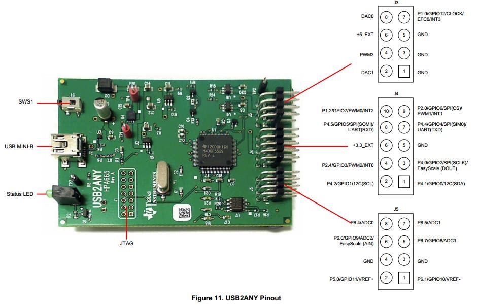
  • I have found this diagram for the USB2ANY output pins. I just want to confirm since I'm using SPI write to LMK and LMX registers, so I should connect Pin3,5,7 and 9 of J4 to my LMK and LMX SCLK, MOSI, CS and GND right? I'm just confused how should I use the Pin configuration panel on the codeloader

  • You shouldn't have to change the port setup in CodeLoader. Make sure the pin configuration is as shown in evaluation board instructions. What is displayed is a diagram of the pins are configured. When using USB2ANY the Clock/Data/LE (LE is CS* also) are actually forced and don't respond to changes. The other GPIO can be changed however.

    Be aware that the USB2ANY documentation which shows pin 1. However in practice, when plugging a cable in, because of the way it is keyed is backward. Please refer to the pin out of the SPI Header from the eval board instructions vs. the above diagram when using keyed connector.

    The key items for connection are CLK, MOSI (Data), CS (LE), and GND. Also be sure that the RESET pin is not held high to allow programming. These are the basic requirements for communication/programming.

    73,
    Timothy
  • angela zhou said:
    Thank you for your documents. I think the LMK chip might be damaged, and that might be the reason it doesn't output correct frequencies. So I decided to continue my experiments on the LMK04828 and LMX2581 from ADC12J4000EVM, since on this evaluation board it has the option to configure LMK and LMX externally via SPI. So my methodology was if I was able to configure LMK and LMX correctly using external SPI, I should get the exactly same output as using the ADC12J4000 software. So after trying with your suggestions, I encountered two problems:

    If you can program one of the Status_LD outputs to Logic low, then toggle the output using Output (Push-pull) and Output Inverted (Push-Pull), then I expect there is no issue with the device.

    angela zhou said:
    1. previously, I used a FTD4222H USB to SPI chip to configure my LMK and LMX using C++ to read my teand FTD libraries, however I noticed that sometimes clock outputs are half of what I expected, and the status 1, status2 don't light up as its supposed to unless I run the command program several times. It almost seems to me that my program doesn't write into the correct register or value with one try. So I wonder is there any timing specifications on how to program the registers other than it has to follow certain sequences?

    The timing specifications are in the datasheet under section 7.6.  The recommended order is in the datasheet under section 9.5.1.

    For simple lock and output frequencies, you should only have to program each register once.  However for some synchronization/JESD204B setup, it may be required to program some registers more than once.

    angela zhou said:
    2. My second problem is that I decided to try to program my register using the codeloader, but it seems like the SPI connection isn't working as no matter how I change the parameters my chip doesn't respond. The PC to USB2ANY connection is working, since the light flashes when I click ' identify'. But other than that, no matter how I try to load device or run as default mode, there is nothing happening. So do you have a more detailed tutorial or something can guide me on how to configure LMX2581 and LMK04828, how to setup their pin configurations, and maybe what outcomes I could expect to indicate this SPI communication is actually working? The user guide didn't help me too much

    Your firmware is at least version if no message and the identify button works.  Are you able to monitor the CLK/DATA/CS* signals on the PCB when programming?  Setting/clearing the Powerdown bit (on bits/pins page) and observing the current change is a good debug check.  Also changing the Status outputs mode between invert and normal will confirm communication.

    73,

    Timothy

  • Hi Timothy,

    I'm not configuring the LMX2581EVM, I'm configuring the LMX2581 chip on ADC12J4000, so the pin configuration for those two LMX are completely different. And apparently CodeLoader's pin configuration by default is matching with the EVM board. For example:

    both EVM and LMX on ADC has a 10pin header which allows us to use SPI, however, on EVM, pin6 is GND, which matches with what's on CodeLoader, but the LMX2581 on ADC12J4000 has a GND at Pin9. Thus pretty much the pin configuration on CodeLoader is useless to me.

    My solution was to instead of using the 10pin ribbon, I made four wires that directly connect between USB2ANY and LMX on ADC12J4000 for SCLK, CS, MOSI and GND. However sometimes I could configure the LMX properly but sometimes not even with the same configuration. Could you tell me if my setup is correct?

    Thank you
    Angela