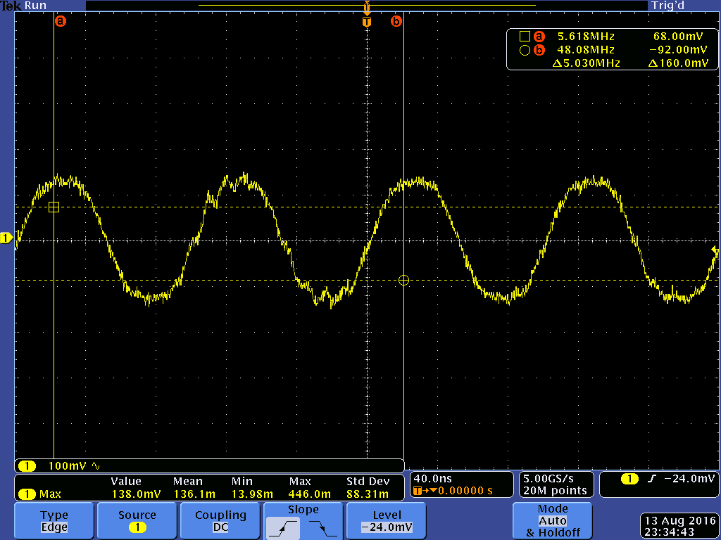
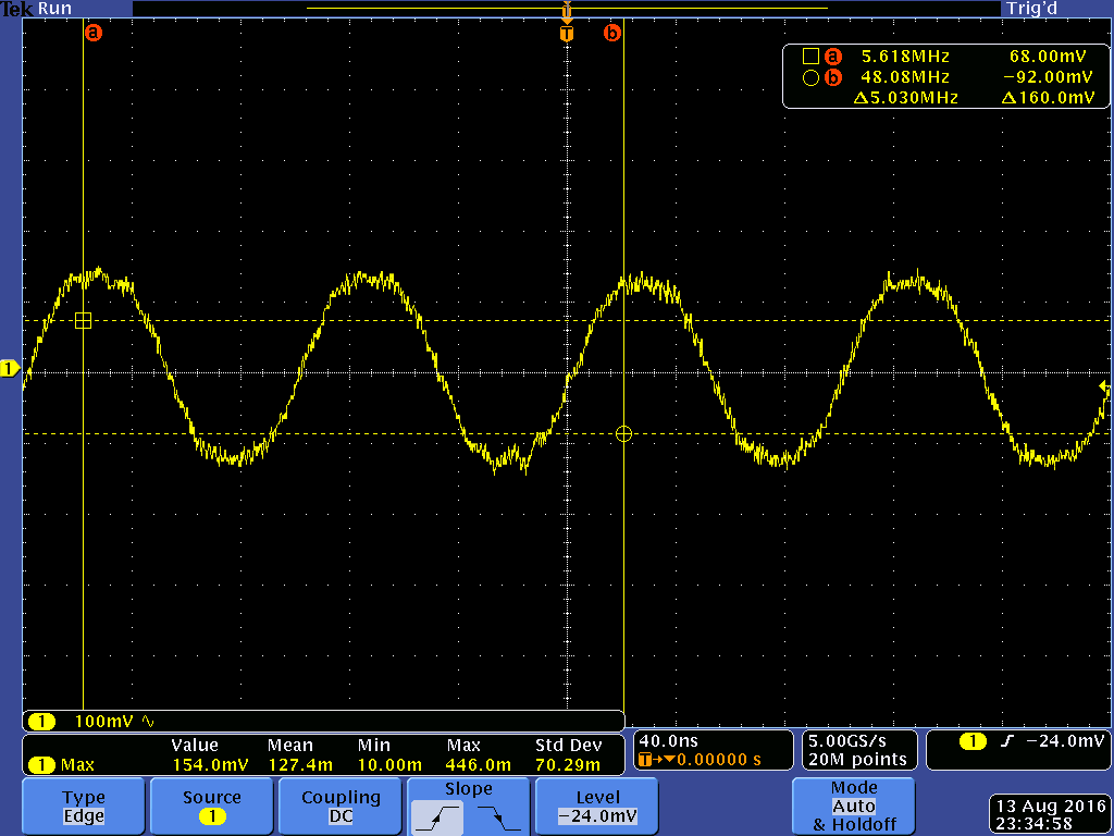
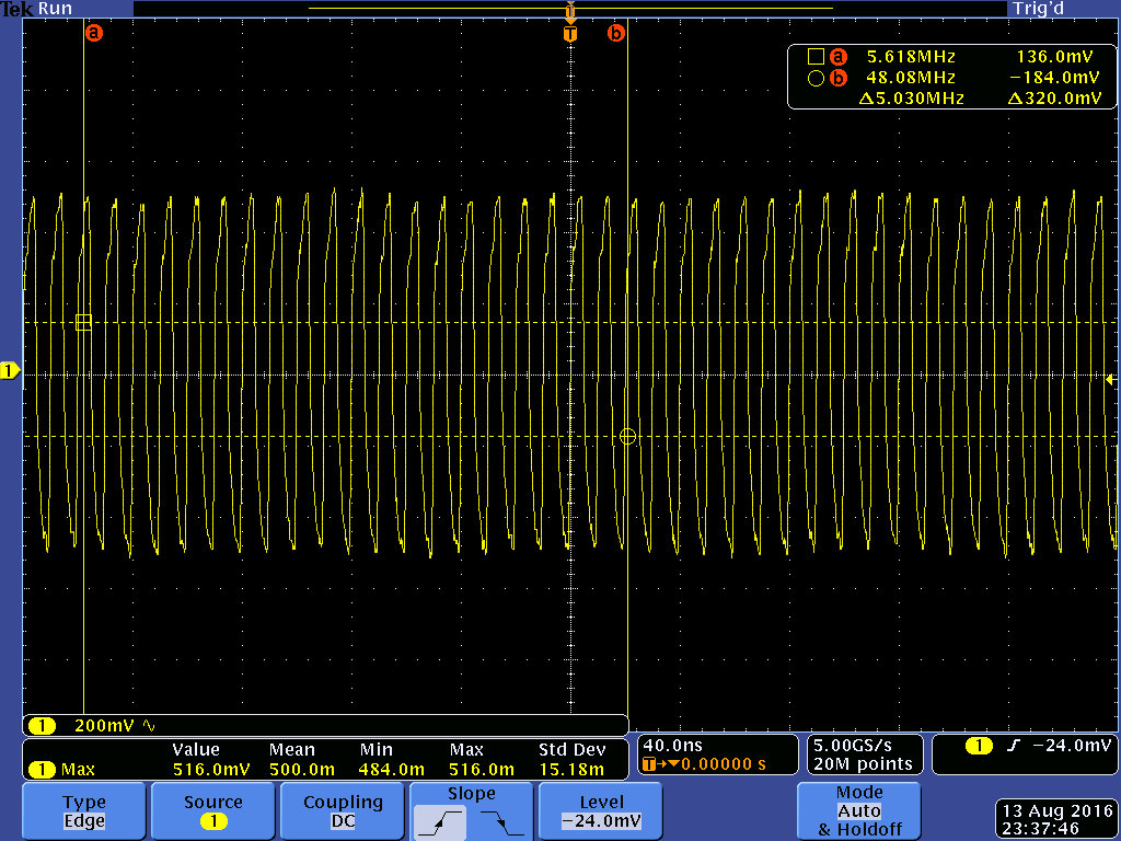
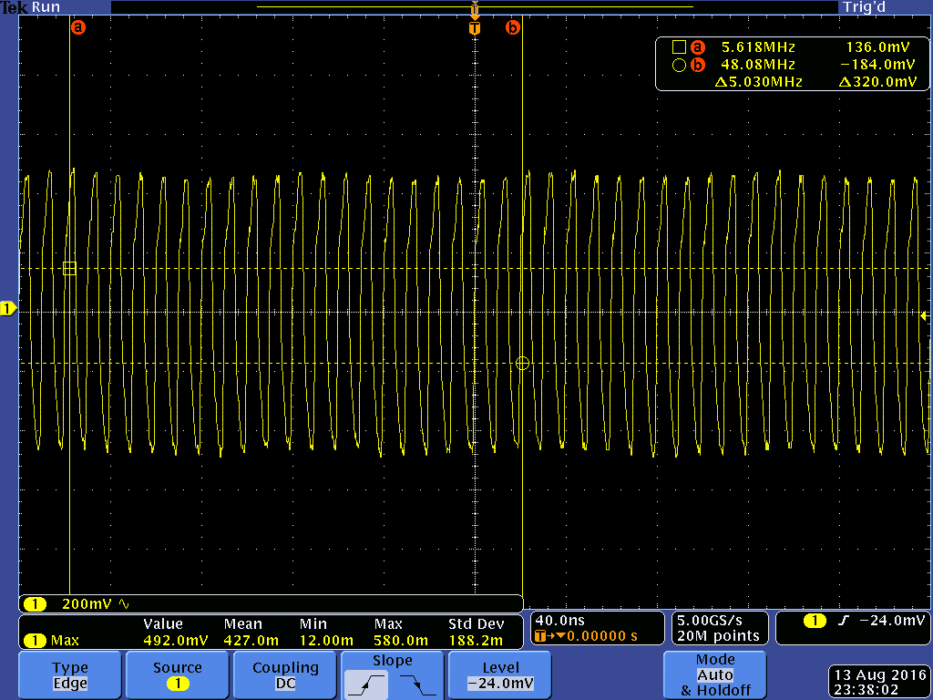
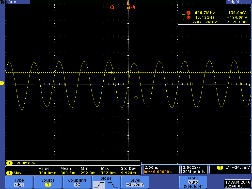
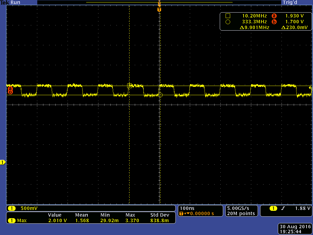
I had a PLL design that previously worked (see the thread 'CDCE72010 PLL fails to lock on FMC150 board'), but the design stopped working after a few weeks. I checked the board for signs of damage near the VCXO and there does not seem to be an issue. The original (working) register settings for an external 10MHz clock source were as follows:
Reg 0 = 683C038
Reg 1 = 6800002
Reg 2 = 8380000
Reg 3 = 6800002
Reg 4 = E980000
Reg 5 = 6800000
Reg 6 = 6800000
Reg 7 = 8380001
Reg 8 = 6800001
Reg 9 = 68050CC
Reg A = 02FC07C
Reg B = 00001C8
Reg C = 0000180
I have also tried these settings:
reg[0x0] = 0x683C0F8;
reg[0x1] = 0x6800002;
reg[0x2] = 0x8380000;
reg[0x3] = 0x6800002;
reg[0x4] = 0xE980000;
reg[0x5] = 0x6800000;
reg[0x6] = 0x6800000;
reg[0x7] = 0x838003A;
reg[0x8] = 0x6800001;
reg[0x9] = 0x68050CC;
reg[0xA] = 0x0BFC07C;
reg[0xB] = 0x0000080;
reg[0xC] = 0x0000180;
Both of which work in the spreadsheet, but not on the real board.
Any suggestions on how to debug this problem?
-Joe Kujawski


