


Other Parts Discussed in Thread: LMK00101
Hi Team,
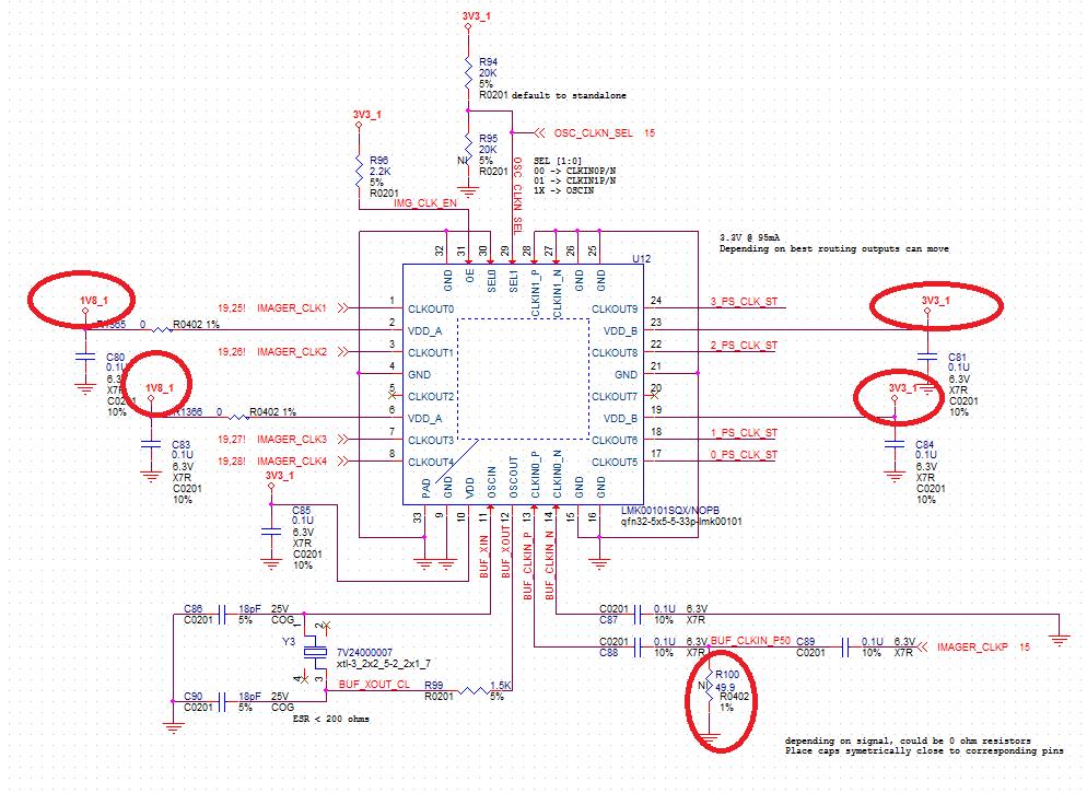
Could you help review the LMK00101 schematic as below?
Their application is outputting below clock with voltage as below
IMAGER_CLK1->1.8V
IMAGER_CLK2->1.8V
IMAGER_CLK3->1.8V
IMAGER_CLK4->1.8V
0_PS_CLK_ST->3.3V
1_PS_CLK_ST->3.3V
2_PS_CLK_ST->3.3V
3_PS_CLK_ST->3.3V
And for R100 originally it is for single end input RC filter, but customer found the signal is better after remove R100, without R100 should be ok right?
Thanks
Sam
