This thread has been locked.

If you have a related question, please click the "Ask a related question" button in the top right corner. The newly created question will be automatically linked to this question.

CDCM7005 unable to lock

Other Parts Discussed in Thread: CDCM7005

Hello,

While using a custome prototype board. I am unable to have a lock on the clock while having a reference 48Mhz clock and a 48Mhz output unless I am using Cycle Slip Lock Window. However it doesn't seem to be locking as I am not able to see the lock between the input clock and the CDC output clock.

I am using the passive loop capacitors and resistor values that are given as example in the datasheet.

The values that I used in the PLL are the ones shown bellow: 

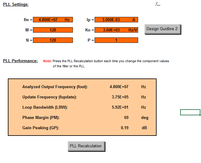
LBW seems a bit low but my guess is that shouldn't be a problem. 

I am using the a 48Mhz VCXO with:

Control Voltage Tuning Slope - 40 ~ 75 ppm/V

BW - 10 kHz

The settings that I am using for the CDCM7005 configuration are the following:

word 0: 0x4007F1FC

word 1: 0x28000001

word 2: 0x500000F2

word 3: 0x0000024B

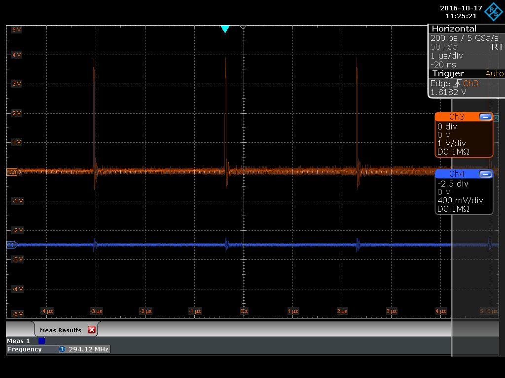
Using the test configuration to see the internal clocks I don't see the VCXO clock (in blue bellow)

Ch3 (orange): STATUS REF

Ch4 (blue): VCXO STATUS

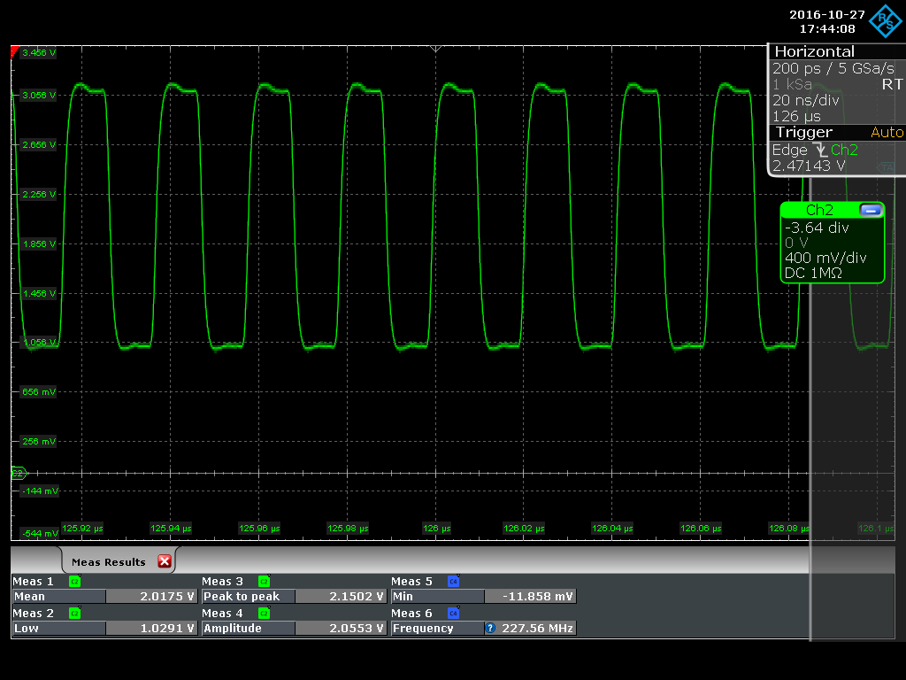
I seem to have the right values for a LVCMOS VCXO. The conditioning circuit is bellow as well as the measured VCXO input in the CDC

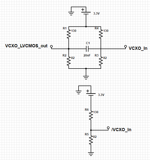
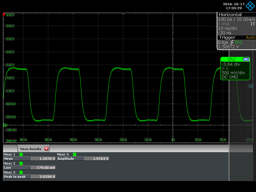
The input VCXO input on the CDC is the following:

The outputs are toggling at the correct frequency although there is no lock.

Thank you

  • What is the tuning voltage to the VCXO? Is it railed?

    Now you appear to be getting a clock with the Vcc - 2 V setting on VCXO_IN and /VCXO_IN biasing. However when you re-bais the common mode to 1.3 V, you're lower than typical center voltage of an LVPECL signal. LVPECL as measured single ended on one output to ground can swing from 1.6 V to 2.4 V on a single output, resulting in 2.0 V as the middle voltage. Flipping the 82 and 130 ohm resistor divider gives you about 2 V. You'll notice that the CDCM7005 provides VBB at Vcc - 1.3 V (about 2.0 V) to bias the /VCXO_IN for use with single ended signals. I think you should swap your resistors to bias your input closer to 2 V Vcm.
    - I notice no tie dot between R3-R4 and C1-VCXO_IN; I presume that's a illustration error?

    Since you are getting output clocks, that suggests VCXO_IN path is working, however perhaps there is some issue with your REF path? Is the proper reference selected (PRI vs. SEC); Is the input meeting the LVCMOS signal requirements?

    73,
    Timothy
  • Hi Timothy

    The tuning voltage is 0 to 3.3V.

    I have changed the resistors as you've suggested but I still haven't managed to achieve lock. The signal has the following waveform.

    The signal seems to be within the parameters of the datasheet.

    About the R3 and R4 they are connected, as you've said it's an ilustration error.

    The REF path is fine, I can see that the correct reference is being used through the status ref pin. They are both LVCMOs going directly to the CDC.

    Tiago

  • When you say 0 to 3.3 V, that means it is erratically between 0 to 3.3 V? I would have expected a constant voltage, railed high, low, or somewhere between (locked).

    When you say unlocked, if Vtune is centered, the device could indeed be locked, but lock report not properly reporting lock.

    73,
    Timothy
  • Hello Timothy

    My mistake. Hard to tell what's the value of Vtune since it seems that by measuring I am changing the control loop characteristics. However I can see that it is at 3V when I start the measure and going down while I have either a probe or an oscilloscope measuring.

    Another thing that I remembered is that maybe I failed in the calculation of the passive loop characteristics. I am using the VCXO in the datasheet www.foxonline.com/.../FVXO_HC73.pdf
    Did I calculated something incorrectly? For example the VCXO sensitivity.

    Thanks Timothy

  • Sounds like your possibly tristated then.  I reviewed your programming in detail and found that:

    /HOLD = 0, meaning CP is tri-stated.  --> This should be changed to 1.

    I also noticed that you have analog lock detect enabled, is this what you really want?

    Hopefully changing /HOLD=1 will result in the device being able to lock.

    73,
    Timothy

  • Thank you for your suggest that wrong bit configuration was indeed the culprit. I have the circuit locking as it should.

    Analog lock detect is enabled because I am using the hold-over function.

    Thank you for your great support