This thread has been locked.

If you have a related question, please click the "Ask a related question" button in the top right corner. The newly created question will be automatically linked to this question.

CDCE62005 Question..

Other Parts Discussed in Thread: CDCE62005

Hello,

We have currently implemented the CDCE62005 in two different ways. One with the Power Down pin tied to VCC_OUT (in this configuration the synthesizer becoming unlocked around 30% of the time), whereas in another configuration the power down pin is connected to the FPGA (the pin is pulled down during power up and then driven high once the FPGA is configured) they don’t see the issue (I can provide schematics if you connect with me on e2e or I can also email them). 

Seeing as one of our TI reference designs (TSW6011 EVM) also ties Power Down to VCC_OUT, I’m wondering if issues have ever been seen with that design or if maybe their problem stems from something else?

I interfaced previously on this with another person from the clocking team and they asked us to add 0.1uF of capacitance on the PDN to solve the issue. In the setup with PDN tied to VCC_OUT, we noticed that VCC_OUT is a 3.3V regulated supply with already 770nF of capacitance. We wanted to ask if we could try an LC circuit to isolate the capacitance in efforts to hold PDN low, longer? In table 4 of the datasheet it mentions after the power supply reaches approx. 2.35V, the contents of the EEPROM are copied into the Device Registers. Is this the voltage level the PDN considers a low-to-high transition? 

Do you have any other comments on this or have you ever heard of this occurring before?

  • Update:

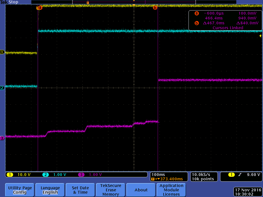
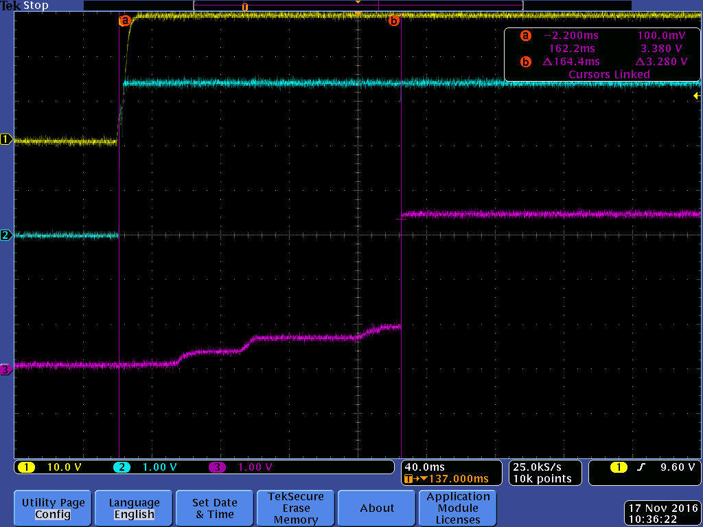
    Another characteristic the customer is noticing is that their supply is not monotonic and that it actually progressively steps up as other supplies turn on (supply to synthesizer is turned on by FET). They were able to reduce the turn-on time from when the main 3.3V supply turns on to when the supply to the synthesizer turns on (please see scope shots below, first is long power up, second is short) but I’m guessing this could still be a cause of the instability/loss of lock they’re seeing?

    On the other hand, they have made a second observation with their implementation where PDN Is tied to VCC_OUT. They’ve monitored/captured the SPI bus communications to the device. The current FPGA control of the CLK and MOSI signals are held low  when not programming/interfacing with the synthesizer. When monitoring the lock signal (out of the synthesizer), it is going low when the CLK signal is pulled low after programming (latch enable remains high). In some reprogramming cases the lock signal recovers almost immediately, in others the lock signal never recovers as seen below.

    In  this implementation they have to power cycle to recover the lock signal. They assume if they could toggle the PDN it would recover as well. When implementing a CLK control that keeps it pulled high when not programming/interfacing with the synthesizer, the lock signal remains high (never dropping).

    This brings us to the next question since they aren’t sure how the CLK signal should be handled when not programming the synthesizer. The timing waveform on page 11 of datasheet depicts the signal starting low (when performing a SPI write) but the signal description on page 5 mentions this signal has in an internal pull-up when not connected. They say they do seem to maintain a more stable lock signal when the CLK signal is pulled high when not interfacing with the synthesizer.

    Any feedback you can provide on the observations is very appreciated.

  • Hello Amanda,
    can you please clarify which of the scope channels is the 3.3V of the CDCE62005?
    SPI_LE must be at static high level before the !PDN goes to high level for the EEPROM loading into the registers and VCO calibration being started.
    What is the input reference clock? Is this clock already powered and provides stable frequency?
    When a crystal is used which model is used?

    Thanks!

    Best regards,
    Patrick
  • Hello Patrick,

    Thanks for your quick response. 

    "can you please clarify which of the scope channels is the 3.3V of the CDCE62005?"

    -The Legend for the scope is as follows (my apologies, I forgot to include):

    Channel 1: 28V supply into the board
    Channel 2: Main 3.3V
    Channel 3: 3.3V Supply for Clock Synthesizer

    "What is the input reference clock?"

    - 10MHz TCXO

    "Is this clock already powered and provides stable frequency?"

    - The reference CLK and Synthesizer are powered up at the same time. 

    "When a crystal is used which model is used?"

    - Connor Winfield - M622-010.0M

    Sorry I should've clarified but the CLK signal that the latter portion of my most recent response was referring to is the SPI CLK which comes from the FPGA and runs at 5MHz.

    Can you comment on what should be done with SPI_CLK signal when the synthesizer is not being programmed?

    Thanks so much for looking at this!

    -Amanda 

  • Hello Amanda,
    the schematic snippet (sent by mail) looks ok. Can you please share the registers settings with me?
    The SPI CLK should be 'low idle'.

    Thanks!

    Best regards,
    Patrick
  • Hello Patrick,

    Thanks for your continued help with all this. The register settings are as follows:

    Reg 0000 "81040320"
    Reg 0001 "EB840321"
    Reg 0002 "811E0302"
    Reg 0003 "EB800303"
    Reg 0004 "81800314"
    Reg 0005 "38100A75"
    Reg 0006 "806E49E6"
    Reg 0007 "BD8875F7"

    -Amanda
  • Hello Amanda,
    thanks for sharing the settings. These are fine. So it seems this is related to our startup getting confused.
    As you mentioned above it will be important to delay the powerdown pin signal and still keep a fairly good slew rate on the rising edge. The FPGA working fine is basically matching that theory.

    Best regards,
    Patrick
  • Hello Patrick,

    Thanks for your response. How much delay do you suggest on the PDN pin and what do you believe is the range we should maintain for the slew rate (this may be given in the datasheet, I'll check)?

    Do you think there is any other way for them to fix what they're seeing without having to use up an FPGA pin (on the PDN pin) as they have been for their current fix? Maybe adding a supervisor so they don't have the stepping and it stays low until it has reached that 2.5V transitional threshold?

    -Amanda

  • Hello Patrick,

    Have you had the chance to look into this as of yet, could you comment?

    -Amanda
  • Hello Amanda,
    as you already wrote. they will have to add a FPGA or MCU to control the startup. When they add a lot of analog delay they will run into the slew rate + noise issue.
    I think adding a cap of  2.2nF to 4.7nF should introduce enough delay when a MCU is not an option.

    Best regards,
    Patrick