This thread has been locked.

If you have a related question, please click the "Ask a related question" button in the top right corner. The newly created question will be automatically linked to this question.

What's wrong with my lmk04821 configuration?

Other Parts Discussed in Thread: LMK04821, CODELOADER, TICSPRO-SW

Hello,

In my design I need to supply clocking for a JESD204B interface by using a Arria V FPGA to configure lmk04821.

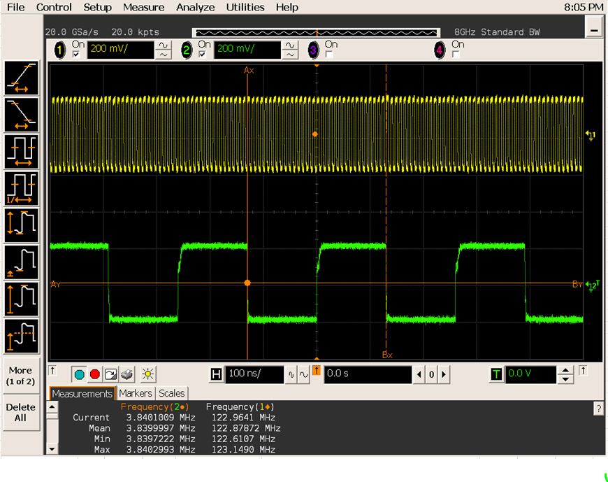
According to Key Points to Setting up SYNC & SYSREF on LMK0482x with CodeLoader.pdf, i write a configuration file as below but the clock output is wrong.(left is dclk output and right is sysref outout)

Can you tell me whats wrong and how can i solve my problem? Thank you.


The  configuration sequence is shown as below:

    localparam  R0  = 24'h0000_80,
                R1  = 24'h0000_00,
                R2  = 24'h0002_00,
//-----------step 1 Setup Clock Outputs-------------------------//
//Set SDCLKoutY_MUX = SR Select SYSREF source  for SDCLKoutY.//
//Set DCLKoutX_DDLY_PD = 0 & SYSREF_DDLY_PD = 0//


                R3  = 24'h0100_08,
                R4  = 24'h0101_55,
                R5  = 24'h0103_01,
                R6  = 24'h0104_22,
                R7  = 24'h0105_00,
                R8  = 24'h0106_71,
                R9  = 24'h0107_01,
                R10 = 24'h0108_0A,
                R11 = 24'h0109_55,
                R12 = 24'h010B_00,
                R13 = 24'h010C_22,
                R14 = 24'h010D_00,
                R15 = 24'h010E_71,
                R16 = 24'h010F_11,
                R17 = 24'h0110_0A,
                R18 = 24'h0111_55,
                R19 = 24'h0113_00,
                R20 = 24'h0114_22,
                R21 = 24'h0115_00,
                R22 = 24'h0116_71,
                R23 = 24'h0117_11,
                R24 = 24'h0118_08,
                R25 = 24'h0119_55,
                R26 = 24'h011B_00,
                R27 = 24'h011C_22,
                R28 = 24'h011D_00,
                R29 = 24'h011E_71,
                R30 = 24'h011F_11,
                R31 = 24'h0120_08,
                R32 = 24'h0121_55,
                R33 = 24'h0123_00,
                R34 = 24'h0124_02,
                R35 = 24'h0125_00,
                R36 = 24'h0126_71,
                R37 = 24'h0127_10,
                R38 = 24'h0128_08,
                R39 = 24'h0129_55,
                R40 = 24'h012B_00,
                R41 = 24'h012C_02,
                R42 = 24'h012D_00,
                R43 = 24'h012E_79,
                R44 = 24'h012F_00,
                R45 = 24'h0130_08,
                R46 = 24'h0131_55,
                R47 = 24'h0133_00,
                R48 = 24'h0134_22,
                R49 = 24'h0135_00,
                R50 = 24'h0136_71,
                R51 = 24'h0137_01,
                R52 = 24'h0138_25,
                R53 = 24'h0139_00,
                R54 = 24'h013A_01,
                R55 = 24'h013B_00,
                R56 = 24'h013C_00,
                R57 = 24'h013D_08,
                R58 = 24'h013E_03,
                R59 = 24'h013F_00,
                R60 = 24'h0140_0D,
                R61 = 24'h0141_00,
                R62 = 24'h0142_00,
                R63 = 24'h0143_01,
                R64 = 24'h0144_FF,
                R65 = 24'h0145_7F,
                R66 = 24'h0146_18,
                R67 = 24'h0147_1A,
                R68 = 24'h0148_02,
                R69 = 24'h0149_42,
                R70 = 24'h014A_02,
                R71 = 24'h014B_16,
                R72 = 24'h014C_00,
                R73 = 24'h014D_00,
                R74 = 24'h014E_C0,
                R75 = 24'h014F_7F,
                R76 = 24'h0150_03,
                R77 = 24'h0151_02,
                R78 = 24'h0152_00,
                R79 = 24'h0153_00,
                R80 = 24'h0154_78,
                R81 = 24'h0155_00,
                R82 = 24'h0156_03,
                R83 = 24'h0157_00,
                R84 = 24'h0158_96,
                R85 = 24'h0159_00,
                R86 = 24'h015A_03,
                R87 = 24'h015B_D4,
                R88 = 24'h015C_20,
                R89 = 24'h015D_00,
                R90 = 24'h015E_00,
                R91 = 24'h015F_0B,
                R92 = 24'h0160_00,
                R93 = 24'h0161_05,
                R94 = 24'h0162_A4,
                R95 = 24'h0163_00,
                R96 = 24'h0164_00,
                R97 = 24'h0165_0A,
                R98 = 24'h0174_05,
                R99 = 24'h017C_15,
                R100= 24'h017D_33,
                R101= 24'h0166_00,
                R102= 24'h0167_00,
                R103= 24'h0168_0A,
                R104= 24'h0169_59,
                R105= 24'h016A_20,
                R106= 24'h016B_00,
                R107= 24'h016C_00,
                R108= 24'h016D_00,
                R109= 24'h016E_13,
                R110= 24'h0173_00,
                R111= 24'h1FFD_00,
                R112= 24'h1FFE_00,
                R113= 24'h1FFF_53,


//-----------step 2 Power up SYSREF and prepare SYNC path to Dividers-------------------------//


                R114= 24'h0143_11,//SYNC_EN = 1   SYNC_MODE = Sync Pin;SYSREF_MUX = Normal SYNC
                R115= 24'h0140_08,//SYSREF_PD = 0 SYSREF_PLSR_PD = 0
                R116= 24'h0144_00,//SYNC_DISSYSREF = 0 SYNC_DISX = 0
                
                R117= 24'h0106_70,//SDCLKoutY_PD = 0
                R118= 24'h010E_70,
                R119= 24'h0116_70,
                R120= 24'h011E_70,
                R121= 24'h0126_70,                     
                R122= 24'h012E_78,
                R123= 24'h0136_70,
//-----------step 3 Reset SYSREF -------------------------//  

                                      
                R125= 24'h0143_91, //SYSREF_CLR = 1                       
                R126= 24'h0143_11, //SYSREF_CLR = 0


 //-----------step 4 Reset SYSREF -------------------------// 

                              
                R127= 24'h0143_31,//SYNC_POL=1                    
                R128= 24'h0143_11,// SYNC_POL=0


 //-----------step 5 Disable SYNC/SYSREF Path from Resetting Dividers-------------------------//  

                      
                R129= 24'h0144_FF, //SYNC_DISSYSREF = 1;SYNC_DISX = 1


 //----------- step 6 Set Desired SYSREF Generation Mode - Pulsed -------------------------//         

                     
                R130= 24'h0139_03,// SYNC_MODE = SPI (Pulser)                                
                R131= 24'h0143_11;//SYNC_MODE = Pin (Pulser)

  • Something different now. There is only correct DCLK output but nothing with SDCLK.

    What is the problem?

    Need your help. Thanks!

  • Hello,
    I expect we'll be able to have an answer to you by tomorrow. However you may find the ticspro-sw EVM software to be improved and assist you better in programming the device.

    73,
    Timothy
  • Hi,
    The newly configuration sequence is as below.
    Still, DCLK output is correct but there is nothing with SDCLK.
    I don't know why and hope to hear from you soon. Thanks a lot!


    //********************signal declarations***************

    localparam RegNum = 140;
    localparam R0 = 24'h0000_80, //Reg 0x000, RESET=1, 3-wire mode enable. The reset bit is automatically cleared.
    R1 = 24'h0000_00,
    R2 = 24'h0002_00, //bit 0: 0--> normal ooperation; 1--> powerdown
    //----------------Device Clock and SYSREF Clock Output Controls------------------
    // DCLKout0, SDCLKout1---->JESD_REFCLK
    R3 = 24'h0100_08, //R100,R108,R110,R118,R120,R128,R130//-> DCLKoutX_DIV
    R4 = 24'h0103_00, //R103,R10B,R113,R11B,R123,R12B,R133, //-> DCLKoutX_MUX
    R5 = 24'h0105_00, //R105,R10D,R115,R11D,R125,R12D,R135, //SDCLKoutY_ADLY_EN, SDCLKoutY_ADLY
    R6 = 24'h0107_11, //R107,R10F,R117,R11F,R127,R12F,R137,
    // DCLKout2, SDCLKout3---->DCLKout2, SDCLKout3: Clock for FPGA DDR3 controllers
    R7 = 24'h0108_0A, //0A Divider Value=10
    R8 = 24'h010B_00, //
    R9 = 24'h010D_00,
    R10 = 24'h010F_11,
    // DCLKout4, SDCLKout5---->DCLKout4: 100 MHz Clock for lmx pll; SDCLKout5: enable
    R11 = 24'h0110_0A, //Divider Value=10
    R12 = 24'h0113_00,
    R13 = 24'h0115_00,
    R14 = 24'h0117_11,//LVDS output, enable LVDS SDCLKoutY
    // DCLKout6, SDCLKout7---->DCLKout6: CLK for FPGA, 125MHz, LVDS
    R15 = 24'h0118_08, //Divider Value=1
    R16 = 24'h011B_00,
    R17 = 24'h011D_00,
    R18 = 24'h011F_11, // LVDS output format,enable LVDS SDCLKoutY
    // DCLKout8, SDCLKout9---->FPGA_CLK- 100MHz
    R19 = 24'h0120_0A,
    R20 = 24'h0123_00,
    R21 = 24'h0125_00,
    R22 = 24'h0127_11,
    // DCLKout10, SDCLKout11---->Powerdown
    R23 = 24'h0128_0F,
    R24 = 24'h012B_00,
    R25 = 24'h012D_00,
    R26 = 24'h012F_00,
    // DCLKout12, SDCLKout13---->test 100MHz
    R27 = 24'h0130_0A,
    R28 = 24'h0133_01,
    R29 = 24'h0135_00,
    R30 = 24'h0137_11, //pll
    //---------------------SYSREF, SYNC, and Device Config---------------------------
    R31 = 24'h0138_25, // selects the clock distribution source, and OSCout parameters
    R32 = 24'h0139_00, // SYSREF_MUX = 0(a)
    R33 = 24'h013A_01, // SYSREF_DIV = 256(c)
    R34 = 24'h013B_00,

    R35 = 24'h013F_00, // controls the feedback feature
    R36 = 24'h0141_00, // enables dynamic digital delay for enabled device clocks and SYSREF when DDLYd_STEP_CNT is programmed
    R37 = 24'h0142_02, // sets the number of dynamic digital delay adjustments occur

    R38 = 24'h0145_7F, // Always program this register to value 127
    //---------------------CLKin Control----------------------------------------------
    R39 = 24'h0146_18,// CLKin enable and type controls
    R40 = 24'h0147_0E,//Pin Select Mode
    R41 = 24'h0148_00,// CLKin_SEL0 controls
    R42 = 24'h0149_40,// CLKin_SEL1 controls and register readback SDIO pin type
    R43 = 24'h014A_0E,// control of the RESET pin
    //-------------------------Holdover----------------------------------------------
    R44 = 24'h014B_06,
    R45 = 24'h014C_00,
    R46 = 24'h014D_00,
    R47 = 24'h014E_00,
    R48 = 24'h014F_7F,
    R49 = 24'h0150_03,
    R50 = 24'h0151_02,
    R51 = 24'h0152_00,
    //-------------------PLL1 Configuration--------------------------------
    // value of the CLKin0 R divider
    R52 = 24'h0153_00,
    R53 = 24'h0154_03,
    // value of the CLKin1 R divider
    R54 = 24'h0155_00,
    R55 = 24'h0156_03,
    // value of the CLKin2 R divider
    R56 = 24'h0157_00,
    R57 = 24'h0158_03,
    // N divider value for PLL1
    R58 = 24'h0159_00,
    R59 = 24'h015A_03,

    R60 = 24'h015B_D7,//controls the PLL1 phase detector ???
    //value of the PLL1 DLD counter
    R61 = 24'h015C_20,
    R62 = 24'h015D_00,
    //delay value for PLL1 N and R delays
    R63 = 24'h015E_00,
    R64 = 24'h015F_0B,//configures the PLL1 LD pin
    //-------------------PLL2 Configuration---------------------------------
    // value of the PLL2 R divider
    R65 = 24'h0160_00,
    R66 = 24'h0161_01,// PLL2_R=1

    R67 = 24'h0162_44,// PLL2 N Prescaler=2
    R68 = 24'h0163_00,
    R69 = 24'h0164_00,
    R70 = 24'h0165_05,

    R71 = 24'h0171_AA,
    R72 = 24'h0172_02,
    R73 = 24'h0174_05, //VCO1_DIV
    R74 = 24'h017C_15,
    R75= 24'h017D_33,

    R76= 24'h0166_00,
    R77= 24'h0167_00, // PLL2_N=5
    R78= 24'h0168_05,
    R79= 24'h0169_59,
    //value of the PLL2 DLD counter
    R80= 24'h016A_20,
    R81= 24'h016B_00,

    R82= 24'h016C_00,
    R83= 24'h016D_00,
    R84= 24'h016E_13,

    R85 = 24'h0173_00,
    //------------------------------------------------------------------------------------------------------------------------------
    R86 = 24'h0143_91, // //SYNC_POL=0, SYNC_EN=1,SYNC_MODE=1 SYSREF_CLR = 1.//是否应该往后放(a)(e)111111111111

    R87 = 24'h010E_70, //-> SDCLKoutY_PD =1 DCLKoutX_DDLY_PD=0 CLKoutX_Y_PD=0(enable)(d)2222222222
    R88 = 24'h0116_70,//-> SDCLKoutY_PD =1 DCLKoutX_DDLY_PD=0 CLKoutX_Y_PD=0(enable)
    R89 = 24'h0106_70, //R106,R10E,R116,R11E,R126,R12E,R136,//-> SDCLKoutY_PD =0 DCLKoutX_DDLY_PD=0 CLKoutX_Y_PD=0(enable)
    R90 = 24'h011E_70,//-> SDCLKoutY_PD =1 DCLKoutX_DDLY_PD=0 CLKoutX_Y_PD=0(enable)
    R91 = 24'h0126_70,//-> SDCLKoutY_PD =1 DCLKoutX_DDLY_PD=0 CLKoutX_Y_PD=0
    R92 = 24'h012E_F9,//-> SDCLKoutY_PD =1 DCLKoutX_DDLY_PD=1 CLKoutX_Y_PD=1(PD)
    R93 = 24'h0136_70,//-> SDCLKoutY_PD =1 DCLKoutX_DDLY_PD=0 CLKoutX_Y_PD=0

    R94 = 24'h0140_00, //SYSREF_GBL_PD=1, SYSREF_PD=0,SYSREF_DDLY_PD=0, SYSREF_PLSR_PD=1 while in continue mode -> 01
    R95 = 24'h013E_01, // SYSREF_PULSE_CNT=1

    R96 = 24'h010E_70, //-> SDCLKoutY_PD =0 DCLKoutX_DDLY_PD=0 CLKoutX_Y_PD=0(enable)
    R97 = 24'h0116_70,//-> SDCLKoutY_PD =0 DCLKoutX_DDLY_PD=0 CLKoutX_Y_PD=0(enable)
    R98 = 24'h0106_70, //R106,R10E,R116,R11E,R126,R12E,R136,//-> SDCLKoutY_PD =0 DCLKoutX_DDLY_PD=0 CLKoutX_Y_PD=0(enable)
    R99 = 24'h011E_70,//-> SDCLKoutY_PD =0 DCLKoutX_DDLY_PD=0 CLKoutX_Y_PD=0(enable)
    R100 = 24'h0126_70,//-> SDCLKoutY_PD =0 DCLKoutX_DDLY_PD=0 CLKoutX_Y_PD=0
    R101 = 24'h012E_F9,//-> SDCLKoutY_PD =1 DCLKoutX_DDLY_PD=1 CLKoutX_Y_PD=1(PD)
    R102= 24'h0136_70,//-> SDCLKoutY_PD =0 DCLKoutX_DDLY_PD=0 CLKoutX_Y_PD=0

    R103= 24'h0143_91, // //SYNC_POL=0, SYNC_EN=1,SYNC_MODE=1 SYSREF_CLR = 1.//

    R104= 24'h0143_91, // //SYNC_POL=0, SYNC_EN=1,SYNC_MODE=1 SYSREF_CLR = 1.//

    R105= 24'h0101_55, //R101,R109,R111,R119,R121,R129,R131, -> DCLKoutX_DDLY_CNTH, DCLKoutX_DDLY_CNTL
    R106= 24'h0109_55, //Delay Values =Reserved
    R107= 24'h0111_55,
    R108= 24'h0119_55,
    R109= 24'h0121_55,
    R110= 24'h0129_55,
    R111= 24'h0131_55,

    R112= 24'h0104_22, //R104,R10C,R114,R11C,R124,R12C,R134, DCLKoutX_HS, SDCLKoutY_MUX, SDCLKoutY_DDLY, SDCLKoutY_HS//- >SDCLKoutY_MUX
    R113= 24'h010C_22,
    R114= 24'h0114_22,
    R115= 24'h011C_22,
    R116= 24'h0124_22,
    R117= 24'h012C_02,
    R118= 24'h0134_02,

    R119= 24'h013C_00, // set the delay of the SYSREF digital delay value 66666666666
    R120= 24'h013D_08,

    R121= 24'h0144_00, // SYNC_DISSYSREF, SYNC_DISX=0 666666666666 To allow SYNC to effect dividers:
    //------------------- 2 Perform SYNC by toggling SYNC_POL = 1 then SYNC_POL = 0.-------------------------

    R122= 24'h0143_B1, // SYNC_POL=1, SYNC_EN=1,SYNC_MODE=1 SYSREF_CLR = 0
    R123= 24'h0143_91, // SYNC_POL=0, SYNC_EN=1,SYNC_MODE=1 SYSREF_CLR = 0

    //-------------------3 disable SYNC from resetting these dividers.-------------------------

    R124= 24'h0144_FF, //

    //-------------------4 Release reset of local SYSREF digital delay.-------------------------

    R125= 24'h0143_11,// SYNC_POL=0, SYNC_EN=1,SYNC_MODE=1 SYSREF_CLR = 0 SYNC_MODE = 1
    //------------------- 5 Set SYSREF operation -------------------------


    R126= 24'h0139_03, // Now asserting the SYNC pin, or toggling SYNC_POL will result in a series of 2 SYSREF pulses.?

    //-------------------Misc Registers-------------------------

    R127= 24'h1FFD_00,
    R128= 24'h1FFE_00,
    R129= 24'h1FFF_53;
  • Hello,

    I tried the above configuration and was able to successfully program the device.  I didn't try reproducing the exact order that you have, but rather just programmed the final set of registers.  I did have to use 122.88 MHz as a reference frequency because the eval board uses 122.88 MHz VCXO, this resulted in me changing the PLL2 N from 5 to 4 so that it would lock at 2949.12 MHz.

    Is this being tested on more than one board?  Can you use this code to power/power down the device (or toggle an Status_LD pin by using PLL2_LD_TYPE to change output to inverting?).

    Here is the example plot I collect, note the output frequency is changed slightly as my VCO is at 2949.12 MHz.  I think your VCO normally operates at 3000 MHz and would then produce 125 MHz from the output I tested:

    73,
    Timothy

  • From your image above, it appears your SYNC_DISX/SYNC_DISSYSREF bits are not set and the SYSREF divider is resetting itself... but your register map is proper to set register 0x144 = 0xff for final operation.

    73,
    Timothy
  • Thank you for your reply but there is still nothing with my sysref output.

    I wonder if you can give me your whole register configuration file, which contains value and sequence.

    Thanks!

  • Hello,

    Sorry for the delay. Please note that the TICS Pro software (TICSPRO-SW) now supports the LMK04821 directly. You might try clocking SYNC/SYSREF page, then clock 'Continuous' for continuous SYSREF. This may help you get a config to generate SYSREF.

    Ensure your desired SDCLKoutY_DIS_MODE is set to active.

    Then on the Clock Outputs page select "SYSREF" for the output in question and uncheck SDCLKoutY_PD.

    Let me know if you're still having issues.

    73,
    Timothy