This thread has been locked.

If you have a related question, please click the "Ask a related question" button in the top right corner. The newly created question will be automatically linked to this question.

LMX2592: LMX clock out through splitter

Part Number: LMX2592
Other Parts Discussed in Thread: ADC12J4000, LMK04828

Hello,

I'm using the LMX2592 to drive an ADC (ADC12J4000)and a DAC at 2.7GHz. 

The two are driven from the same output of the ADC so my solution is to use 2 resistive splitters (one for RFOUT_p and one for the RFout_n).

The ADC clock is then composed of one of each splitter output. same goes for the DAC.

I'm using PD0030SM resistive splitter (DC-30GHz BW)

1. Is that an adequate solution?

2. can I use a power splitter in stead of resistive? if so, what should be the bandwidth of the splitter?


Regards,

Itai

  • Hi Itai,

    Just wonder why don't you use the second output from LMX2592?
    Although the splitter will work, but there are some drawback:
    - extra cost for the splitter
    - pcb layout becomes annoying
    - slew rate may be reduced because of R-C effect, this may hurt the ADC performance
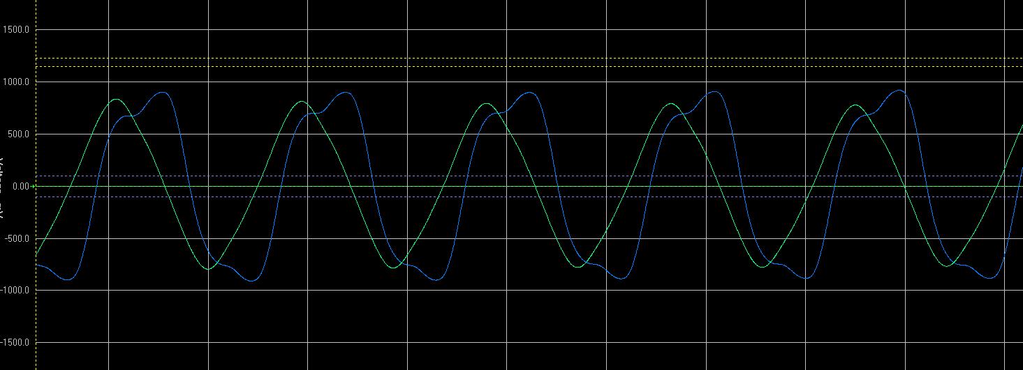
  • Clock 2.7GHz

    The simulation was conducted in Hyperlinx using the LMX & ADC ibis models & Splitter S-parameters model (.S3P).

    PD-0030SM is a very wide band resistive splitter (0-30GHz).

    The relevant nets were exported to Free form schematic.

    - The green wave is the signal when transferred through the Splitter (PD-0030SM).

    - The blue wave is the signal when transferred without the splitters (simply removed from the free form schematic)

    (see attached file for figure)

    It is noticeable that the slew rate is somewhat effected by the splitter.

    Questions:

    1. Do you think such degradation would affect the ADC performance?

    2. Is it possible to roughly predict by how much?

    Best regards,

    Itai

  • Hi Itai,

    I am not familiar with ADC, suggest post this question to the ADC forum.
    BTW, LMX2592 has two outputs, can you use both of them? This way, you don't need the splitter.
  • Hi,

    The second LMX output is used for driving a LMK04828 for clock distribution to other components in the design.

    My design receives 100MHz as input reference clock to the LMX2592. One output of the LMX outputs 2700MHz to an ADC & DAC (split through RESISTIVE SPLITTER ). The second output of the LMX outputs 2700Div4 to the LMK04828. The LMK distributes clocks to the FPGA.

    An optional solution would be to flip the design such that the LMK04828 gets the 100MHz reference, and distributs that to the FPGA as well as the LMX. The LMX then semds the two outputs, one to the ADC and one to the DAC (Similar to TSW40RF80).

    I tend to prefer the original solution for a couple of reasons:

    1. The ADC & DAC clock jitter should be better (less components in the way. LMX only vs. LMK and then LMX)

    2. LMK shows degraded signal amplitude in 2.7GHz.

    3. The ADC & DAC clocks are completely separated from the clocks to the FPGA.

    4. I'm in progressive stages of the layout and changes become difficult at this point :).

    What do you think of the two options?

    Thanks,

    Itai

  • Hi Itai,

    I prefer the other way, i.e. use LMK to provide the reference clock to LMX.
    You can put the 100MHz in the PLL1 of the LMK device, set PLL1 in tri-state mode and shut down unnecessary blocks to save power. PLL1 has a buffered output, you can get a copy of the 100MHz clock, which is still very good to be use as the reference of LMX.