This thread has been locked.

If you have a related question, please click the "Ask a related question" button in the top right corner. The newly created question will be automatically linked to this question.

LMK03328: Need 3.3V LVCMOS O/P specs for LMK03328

Part Number: LMK03328
Other Parts Discussed in Thread: CDCM6208, LMK03318

Hi Team,

Can you provide me with the following specs for LMK03328 & CDCM6208 to compare with the benchmark device for a LVCMOS 3.3V Interface.


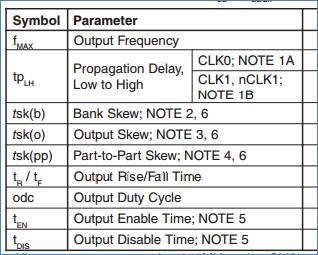
I have found the above information for 1.8V in LMK03328 Datasheet but not for 3.3V.

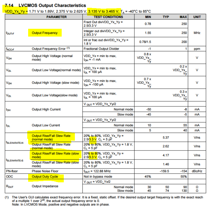
In CDCM6208 Datasheet, I have found info for most of the information customer is requesting for as shown below. Can you provide me with the remaining information.

 Regards,

Praveen

  • Hi Praveen,

    I have followed up with you offline.

    For reference: the LMK03328/LMK03318 LVCMOS levels are fixed (2x 3.3V for STATUS[0:1] and 16x 1.8V for OUT[7:0]) regardless of VDDO voltage so the datasheet specs apply regardless of the VDDO voltage.

    For the CDCM6208, the skew and propagation delay data is given in a separate table of the datasheet. See section 7.19 on page 15: ‘Output Skew and Sync to Output Propagation Delay Characteristics’.

    Finally, the output enable/disable time depends on the method used to enable/disable the outputs. For example, SYNC can be used on both devices to disable and enable all outputs. The delay time would then be a function of the frequency. For LMK03328, see section 10.4.17 on page 49: ‘Output Synchronization’ for an explanation of the enable/disable time. For CDCM6208, see section 10.2.2.9 on page 68: ‘Output Synchronization’. The outputs can also be individually enabled/disabled by writing to registers over I2C but this test method is not defined since I2C timing characteristics would have to be taken into account. There are no individual output enable/disable pins on these devices which is why this specification isn’t defined in the datasheet.

    Regards,

    -Tim