This thread has been locked.

If you have a related question, please click the "Ask a related question" button in the top right corner. The newly created question will be automatically linked to this question.

CDCVF2505 Occasional gradual discharge on the output clock pins when input clock stops

Other Parts Discussed in Thread: CDCVF2505, CDCV304

Hello,

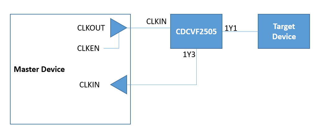
I am working with a board that uses CDCVF2505 for gated clock distribution. The input clock toggles and stops for some period of time for power savings, but we noticed that occasionally the output clock from the buffer does not have a sharp falling edge and instead is decaying slowly. Blue is the input clock and yellow is the output: 

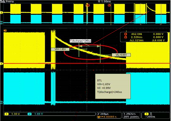
 Is this a known issue for this device? Are there any recommendations for mitigating it? 

Thank you,

ilya

  • Hi Ilya,

    Sorry for the delay in response.

    Could you please send us a copy of your schematics that contains the CDCVF2505? What output are you monitoring?

    Is the input signal always stopped low?

    Regards

    Arvind Sridhar

  • Hi Sridhar,

    Thanks for the response! 

    Let me get the schematics, at the moment I only have a block diagram that I can share:

    We have a master device supplying 33MHz gated clock which then goes to a target device via 1Y1 output and back to the master (to compensate for clock delay on the board) via 1Y3. When clock is gated we always gate it at 0, but looks like the outputs of CDCVF2505 stop at 1 and then decay slowly in some cases. We are monitoring both outputs 1Y1 and 1Y3. Other outputs are not connected on the board. 

  • Thanks Ilya.
    Please bear with us while we work to understand the behavior reported by the customer.
    Regards
    Arvind Sridhar
  • Thank you Sridhar.

    I was able to get the schematics showing the details of other pins. Hope this helps.

    CLK_FB is routed as feedback to the master device and CLK_O goes to the target device in this case. 

    ilya

  • Hi Ilya,

    CDCVF2505 has a frequency detector inside that is RC filter based. If the input frequency is below 10MHz, this block tri-states the output driver. Since the detector is asynchronous, the outputs can be high when the driver gets tri-stated.

    The decay that you observe at the output, is probably the RC delay due to the PCB loading, probe loading and receiver input capacitance (Capacitors in parallel). The combination of the probe impedance and the effective capacitance sets the time constant of the decaying waveform.

    Example: 10M, 30pF leads to a RC time constant of 300us.

    We believe this is what you may be seeing and is expected behavior.

    Regards

    Arvind Sridhar

  • Thank you Sridhar!

    Is there a different delay buffer (not necessarily zero-delay) that is pin compatible with CDCVF2505 (at least for the pins that are used in the schematics above) that would not have this issue? I looked at CDCV304, but doesn't look like it will work due to pin conflict. 

    ilya

  • Hi Ilya,

    Closest we have is CDCV304: www.ti.com/lit/ds/symlink/cdcv304.pdf

    Regards
    Arvind Sridhar