This thread has been locked.

If you have a related question, please click the "Ask a related question" button in the top right corner. The newly created question will be automatically linked to this question.

LMK04828: LMK04828: bypassing PLL2 VCO

Part Number: LMK04828

Hi, Team:

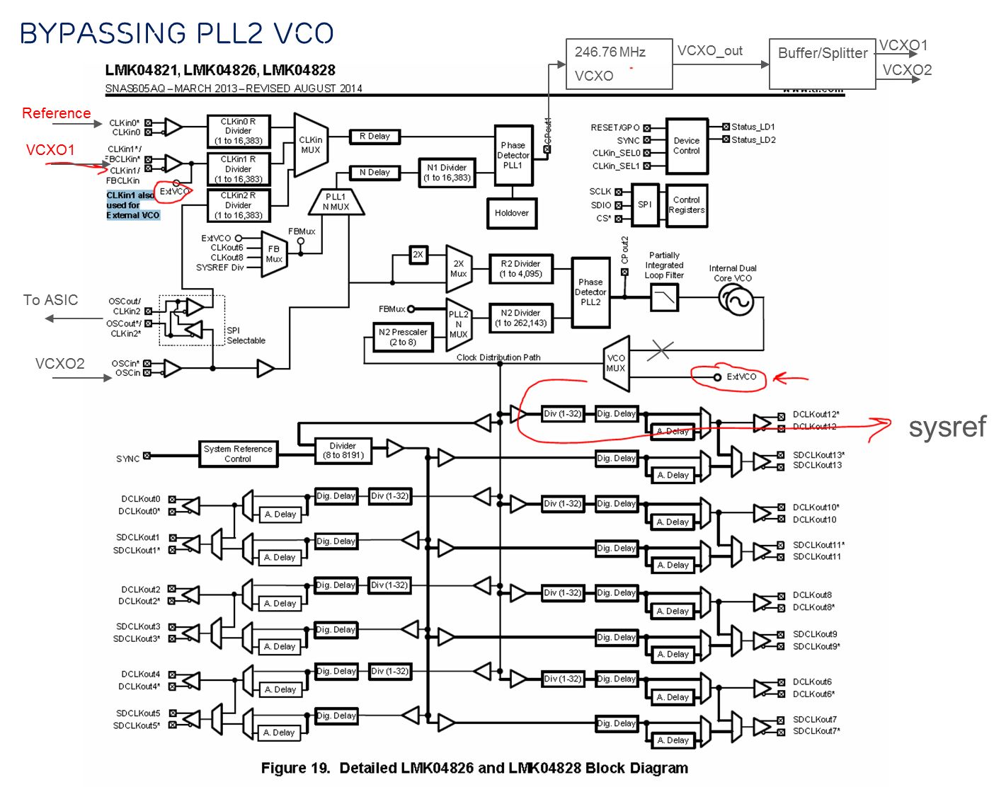
My customer wants to use LMK04828 in bypassing PLL2 and internal VCO mode.

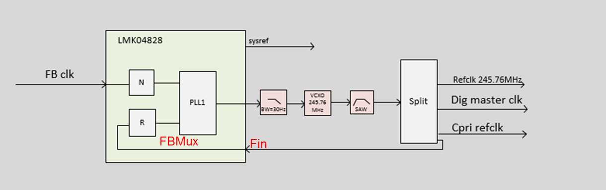
The reference signal is feeded into CLKin0 which is 122.88MHz, external VCXO is connected to Fin or ExtVCO (CLKin1/FBCLKin), FBMux is enabled which routes ExtVCO to PLL1 N divider.

My thinking it should be okay to work, but I would like to get the confirmation and your comments on it. Thank you so much!

  • Hello,

    Normally I would suggest simply provide your reference to OSCin and do single loop with PLL2 providing input to OSCin and the VCXO to CLKin1 as external VCO.

    However maybe you want to use the holdover features of PLL1? I've not tested this, however I think it will work fine. Note you could simplify and not use a buffer/splitter. Connect your VCXO to OSCin. Then connect OSCout to CLKin1 for distribution. The disadvantage is that your device clocks go through two buffer paths. The advantage is that now if providing SYSREF, the timing is more closely aligned... although maybe not a terrible concern at 245.76 MHz.

    Another thought for using PLL2 instead of PLL1 if you want holdover is to connect CPout1 and CPout2 you may still be able leverage the holdover to some extent, some extra work would be required to tri-state CPout2 when entering holdover.

    73,
    Timothy
  • Hi, Timothy:

    Thank you so much!

    Customer won't have the need to use holdover. Can you explain a little bit the timing is more closely aligned if we use PLL1 and connect VCXO to OSCin, then connect OSCout to CLKin1?

    I think if PLL1 is used, we can also simplify the buffer/splitter, and just connect the external OCXO output to CLKin1 for feedback and skip OSCin.

    Best Regards
    Yarn.