Other Parts Discussed in Thread: CODELOADER
Hi Team,
Please advise me on the following questions related to the LMK03328.
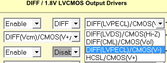
Q1. Can OUTn_P and OUTn_N output the same polarity of clock when outputs are configured in
CMOS mode?
Q2. When 1.8V CMPS outputs are expected, can the VDDO_n be operated with 3.3V supply
or restricted to 1.8V?
The data sheet describes as bellow. This may suggest that to output 1.8V COMS clock,
VDDO_x can be either 1.8V, 2.5V or 3.3V.
~~~~~~~~~~~~~~~~~~~~~~~~~~~~~~~~~~~~~~~~~~~~~~~~~~~~~~~~~~
8.12 1.8-V LVCMOS Output Characteristics (OUT[7:0])(1) VDD_IN / VDD_PLL1 / VDD_PLL2 / VDD_DIG = 3.3 V ± 5%,
VDDO_x = 1.8 V ± 5%, 2.5 V ± 5%, 3.3 V ± 5%, TA = -40°C to 85°C, outputs loaded with 2 pF to GND
~~~~~~~~~~~~~~~~~~~~~~~~~~~~~~~~~~~~~~~~~~~~~~~~~~~~~~~~~~~
Q3. Can you give us the Min and Max value of try-level input pins such as REFSEL, GPIO[3:1] pins.
The datasheet specifies Vim typical value.
However, without MIN and MAX value, you cannot design the application board.
Q4. The device has several outputs (OUT0_P/N to OUT7_P/N) and dedicated power supply pins VDDO_01/23/4/5/6/7.
If some of the outputs are not used the corresponding power pins can be left open or must be
tied to supply?
Q5. The datasheet specifies the power up sequence. Are there any restrictions among VDD_IN, VDD_DIG
VDD_PLL1, VDD_PLL2, VDDO_01/23/4/5/6/7?
Can they be up at nay order as long as they up monotonic, with in 100 ms, and PD up later than
all Power rail?
Mita


