


Other Parts Discussed in Thread: LMK03318,
Hi,
I want to drive the LMK01020 clock input (CLKin0/CLKin0*) with the LMK03318 output driver 0 (OUT0_P/N) configured in AC-LVDS.
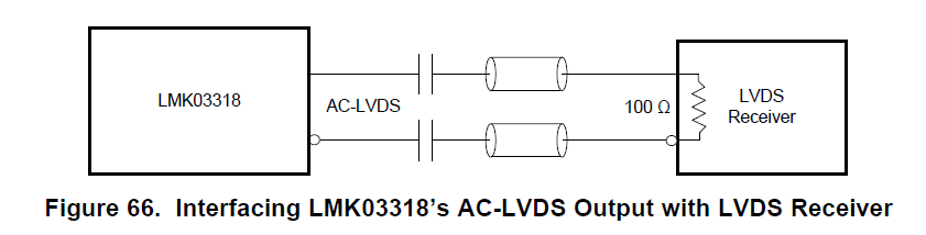
The LMK03318 datasheet (Figure 66 reproduce below) show how to interface the AC-LVDS output:
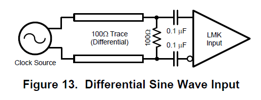
The LMK01020 datasheet state that the CLKin/CLKin* inputs must be AC-coupled and that "the DC blocking capacitors are placed between the termination and the OSCin/OSCin* pins" (p. 16). Furthermore, the LMK01020 datasheet (Figure 13 reproduce below) show how to interface the LVDS clock input:
On the other hand, the post http://e2e.ti.com/support/clocks/f/48/t/219116
From those reading, I understand that the following topologies (Interface #1 and Interface #2) should be valid. My primary concern is for the LMK01020 in the Interface #2 below. For Interface #2, is it right to have a single pair or DC-blocking capacitor between the LMK03318 driver and the termination resistor and not between the termination resistor and the LMK01020 receiver ? This seem to violate the datasheet recommendation.
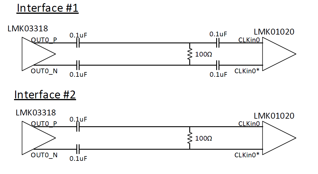
If both interface are valid, which Interface would you recommend for best performance ?
Thank You.
Nicolas.
