This thread has been locked.

If you have a related question, please click the "Ask a related question" button in the top right corner. The newly created question will be automatically linked to this question.

CDCLVP1204: Inquiries about thermal resistance and power consumption

Part Number: CDCLVP1204

Hello,

To check the temperature margin of the product, we calculate the maximum junction temperature using the formula, using the power consumption of the clock buffer IC, the thermal resistance coefficient of the top case, and the top case temperature measured at high temperature.

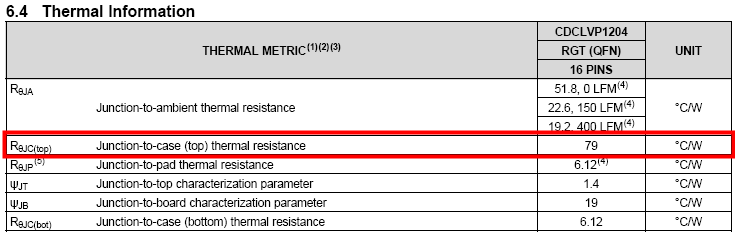
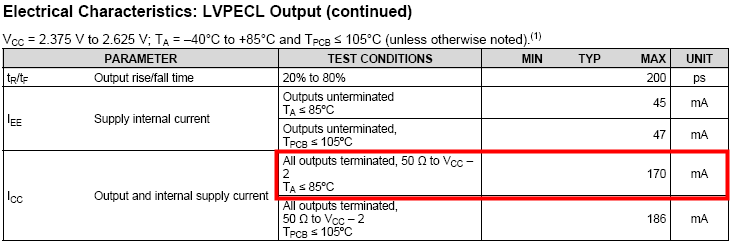
At this time, the amount of power consumption applied to the formula and the thermal resistance coefficient of the top case were refered in the datasheet as follows.

Please check the following items.

(1) The junction-to-case (top) thermal resistance is 79, which is too large compared to other values. Is 79 correct?

(2) To calculate the power consumption value, the maximum power consumption was calculated by multiplying the Icc value of 170 mA by 3.3 V (561 mW). Is it correct to apply 170mA in the same configuration as the clock buffer circuit attached?
thanks,
TS
  • Hello TI,
    Is there anyone can answer my question?
  • The device exposed (bottom) pad should be soldered to your PCB ground land pad for thermal dissipation. So, you may refer to Section 11.3 (Thermal Considerations) in the CDCLVP1204 datasheet to estimate the device's Max junction temperature based on your Max board termperature (Tpcb), which you may assume to be the same as Max ambient temp or higher. Section 11.3 also points out that some power is dissipated in the external load termination resistors (~35mW per loaded output pair), and the device power should exclude the power dissipated in all output load resistors.

    Regards,
    Alan
  • Hello Alan,
    At first, thank you for your answer.
    The bottom pad is naturally designed to be soldered to the PCB, and the intent of the inquiry is that the junction-to-case (top) Is correct.
    The intention was to determine if the thermal resistance factor of the junction-to-case (top) in an operating condition that is soldered to the PCB when the design requirements are fully reflected is true 79.

    And How is power consumption calculated based on the schematic I attached above?
    Comparing the measured values of power consumption and thermal resistance coefficient with the calculated value of 170mA which is MAX value of datasheet, there is almost no margin.

    thanks,
    TS