This thread has been locked.

If you have a related question, please click the "Ask a related question" button in the top right corner. The newly created question will be automatically linked to this question.

LMK03328: Generating Five output frequencies using single IC

Part Number: LMK03328
Other Parts Discussed in Thread: LMK03318, CODELOADER

Hi,

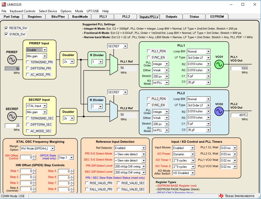
I am using LMK03328 to clock K2H SOC. 

I need to give below clocks ( all LVDS) to the SOC: 

- One 100Mhz 

- Two 125 Mhz

- Two 312.5Mhz

-One 156.25Mhz

- Two 122.88Mhz 

Please let me know is there nay way to generate all these from a single LMK03328 IC.

Thanks & Regards,

Madhu

  • Hi Madhu,

    Yes, LMK03328 is a good solution for this frequency plan. I have created a Webench Clock Architect simulation to show how you could implement this plan, linked below. The simulation shows you what frequencies to set the PLL VCOs to in order to achieve these frequencies. I assumed the input to be a 50MHz input (for example, a 50MHz crystal on SECREF input), doubled to 100MHz using the input frequency doubler for best performance.

    webench.ti.com/.../OpenPublicSharedProject.jsp

    Regards,
    -Tim
  • Hi Tim,

    Thanks for answer.

    In the webench simulation, for 122.88mhz, I could observe spur on the output. Since I am connecting this to the core clock input of K2H device, Is there any chance that this will degrade the SOC functionality?

    Regards,

    Madhu

  • Hi Madhu,

    Currently, Webench simulation of spurs for LMK03328/LMK03318 is inaccurate when the PLL is in fractional mode. In reality there will be much fewer spurs with features such as dithering enabled.

    I will send you a sample CodeLoader GUI configuration file for the LMK03328 next week that is optimized for jitter performance, which should be suitable for K2H clocking.

    Regards,
    -Tim
  • Hi Madhu,

    Please see the attached .mac config file that can be opened with the Codeloader GUI software for LMK03328. It has been optimized for your frequency plan and should be suitable for K2H clocking.

    LMK03328 K2H Example.zip

    Regards,

    -Tim

  • Hello Tim,

    Thanks a lot for sharing the output plan, I am planning to use the same in my design.

    For the input power, I have provided filtering as mentioned below. Please review the same and let me know whether this meets IC requirements:

    - 3.3V is supplied to VDD_IN, VDD_DIG , VDD_PLL1 and VDD_PLL2 pins, using separate ferrite beads and decoupling capacitors.

    - 3.3V is supplied to VDDO_01 and VDDO_23 using a single ferrite bead.

    - 3.3V is supplied to VDDO_4, VDDO_5, VDDO_6 and VDDO_7 pins using a single ferrite bead.

    I request you to go through below image for more details.

    Thanks & Regards,

    Madhu

  • Hi Madhu,

    The power filtering looks mostly ok. My only recommendation is to share ferrite bead/bulk cap between outputs that are generated from the same PLL. From the example config file I sent, OUT0-OUT5 are generated by PLL2 and OUT6-OUT7 are generated by PLL1. Therefore VDDO_01, VDDO_23, VDDO4, and VDDO_5 can share the same ferrite bead and 10uF and 1uF caps. Same goes for VDDO_6 and VDDO_7. When doing layout, be sure to place the 0.1uF close to the device pin.

    The rest of the schematic you shared also looks fine. My only recommendation is to change the loop filter cap values (LF1 and LF2). In the example config file I sent, PLL1 is in fractional mode and PLL2 is in integer mode. The recommended loop filter cap for LF1 fractional mode is 0.033uF and the recommended value for LF2 integer mode is 3300pF. This will improve jitter performance.

    Regards,

    -Tim

  • Hello Tim,

    Thanks for the information.

    Please clarify below points:

    1) Whether there will be any performance issues if I use a 25Mhz crystal ( as given in below image) ?

    2) For another K2H soc, I need only 7 clock inputs. Instead of two 312.5Mhz, only one is used. Whether can i use same configuration by keeping out1 as unused? or Is it better to swap 122.88Mhz and 312.5Mhz so that out7 will remain unused?

    3) How to terminate unused outputs? whether connecting a 100E resisotr between P and N pins would be okay?

    Thanks & Regards,

    Madhu

  • Hi Madhu,

    1. The jitter will slightly increase since the phase detector is running slower, however it should still be able to clock the K2H fine. See attached file: I modified the example config file to use a 25MHz crystal. You can refer to this file since the settings are already optimized.

    2. It is fine to use the same configuration and just terminate the output you are not using.

    3. Yes, for LVDS, unused outputs should either be disabled or terminated with 100 ohms between P and N.

    Regards,

    -TimLMK03328 K2H Example 2.zip

  • Hi Tim,

    In the above configuration suggested, PLL1 output will be 5000MHz and PLL2 output will be 4915.2MHz.

    As of my understanding, PLL1 will be integer mode and PLL2 in fractional mode. So LF1 capacitor must be 3300pF and LF2 capacitor must be  0.033uF.

    Please correct if I am wrong.

    Regards,

    Madhu

  • Hi Madhu,

    That is correct.

    Regards,
    -Tim