

Part Number: CDCE62002
Hi Team,
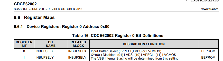
According to Table 16 of the CDCE62002 datasheet (shown below), it looks like writing a ‘1’ to bit 1 (Y) and a ‘0’ to bit 0 (X), so XY= 01, should configure the input as LVDS, according to the Description/Function. The default value in the datasheet and in the EVM SW is XY=01, which is LVPECL (not LVDS), seems to be correct. In the Description/Function column, It looks like either the ‘XY’ should be flipped to be ‘YX’ (preferred), or it should read XY(00) Disabled, (10) LVDS, (01) LVPECL, (11) LVCMOS. Let me know how I should be interpreting this.
Thanks in advance,
Mitchell
